Atomic-scale bottom-up fabrication: Area-Selective Deposition (ASD) of Si-based dielectrics and its application in advanced memory device integration
Leuven | More than two weeks ago
In depth fundamental understanding of atomic layer deposition (ALD) of dielectric materials and surface chemistry to enable innovative and technologically relevant solutions for nano-electronic component miniaturization.
For several decades, NAND flash memory has been the primary technology for low-cost and large-density data storage applications. This non-volatile memory is present in all major electronic end-use markets, such as smartphones, servers, PCs, tablets, and USB drives.
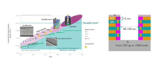
About every two years, the NAND flash industry has been able to substantially improve bit storage density, expressed in terms of increasing Gbit/mm2. To keep up with this trend NAND’s integration transitioned to the third dimension. by stacking cells to form a vertical string. Recently, some of the major players introduced 176-layer 3D-NAND-based products, and this trend of increasing layers is expected to continue in the years to come.
To enable the control of SiO2 blocking oxide and Si3N4 charge trap layer uniformity in this high aspect ratio memory holes, area-selective deposition (ASD) of Si oxide and Si nitride is required. Different routes will be studied to enable ASD, such as plasma-enhanced SiO2 and Si3N4 films selectively deposited on Si3N4 and SiO2 growth areas (GA), respectively and not on the sacrificial Al2O3 non-growth area (NGA).
The general goal of this PhD project is to provide insight in area-selective deposition of Si-based dielectrics, as this is a newly emerging field of research and development and only few research papers have been published. A fundamental study of selectivity and defect formation mechanisms will be an important part of this PhD project together with the advanced characterization of pre-cleaned surfaces, functionalized non-growth surfaces, both growth and non-growth surfaces exposed to gas phase reactants, deposited films, and formed defects.
The final goal of this project is to treasure all the learning gathered on un-patterned surfaces to nano-scale 3D features where the growth and selectivity mechanisms are expected to be different with respect to planar surfaces, due to different incoming surface composition (after etching and post-etching clean) and due to topography/geometry effects.
A great asset offered by Imec is the possibility of getting sub-20 nm patterned features as a result of cutting-edge technology, integration and state-of-the-art materials and 300 mm IC manufacturing equipment.
A cross-team collaboration between the surface and interface preparation, thin film deposition and characterization experts will enable and in-depth understanding of material properties and mechanisms.
Required background: The candidate should have recently obtained a Master in Materials Science, Materials Engineering, Nanotechnology, Chemistry, Physics, Chemical Engineering or Electrical Engineering.
Type of work: 10% literature study, 90% experimental work (depending on the interest of the student a combined experimental/theoretical investigation might be possible)
Supervisor: Annelies Delabie
Co-supervisor: Silvia Armini
Daily advisor: Silvia Armini
The reference code for this position is 2024-166. Mention this reference code on your application form.