Molecular layer deposition of organic–inorganic hybrid films as novel patterning materials
PhD - Gent | More than two weeks ago
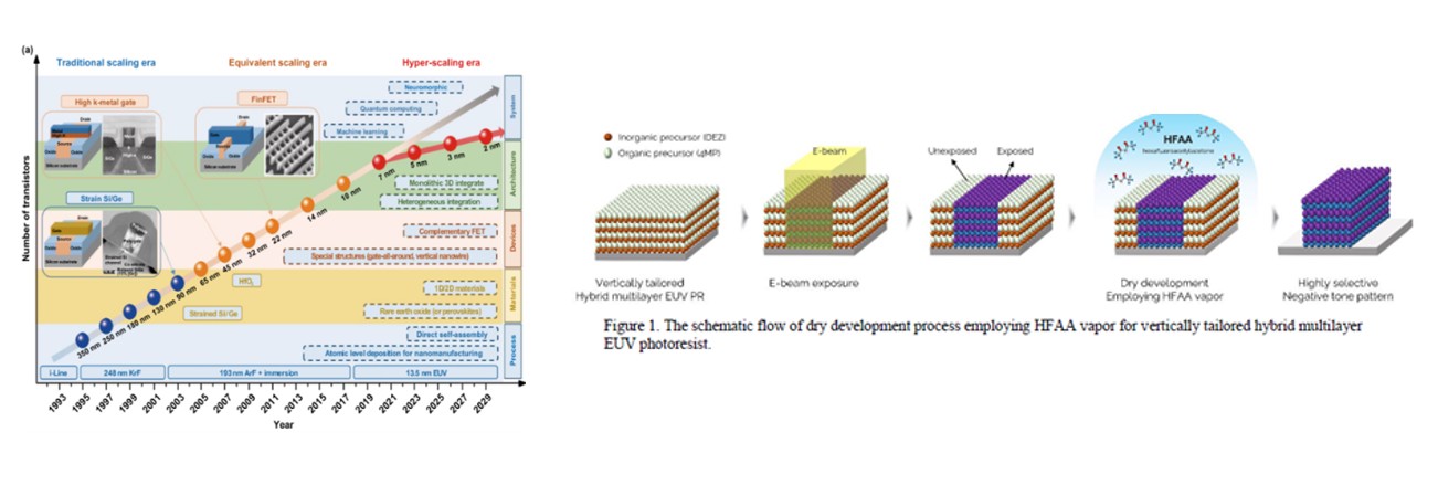
In the past decades, Moore's law has been driving integrated circuit (IC) manufacturing industry to continuously shrink the critical size of transistors down to 7 nm. To continue scaling CMOS technology, both process improvement and advances in patterning materials are crucial. The introduction of extreme ultraviolet (EUV) lithography, a next-generation lithography technology, has driven the need to develop new resists for applications in scaled devices. Metal-based inorganic resists with high EUV absorption efficiencies are suitable EUV resist candidates because they have high etch resistance owing to their excellent mechanical strength even at thin thickness. Organic–inorganic hybrid films grown by molecular layer deposition (MLD) have recently gained increasing attention for their application as organic-inorganic photoresists because of their precise thickness and compositional control below 20 nm using layer-by-layer technology and because they allow overcoming the light dispersion issues observed in wet-deposited inorganic resists. In addition, the novel materials should comply to the following requirements: 1) stability against storage and aging; 2) high resolution below 16 nm pitch and low dose below 60 mJ/cm2; 3) low roughness below 1 nm; 4) high thickness and compositional uniformity, and 5) low stochastic defects < 1 defect/cm2. Therefore, we aim to investigate metal-based organic–inorganic hybrid films deposited via MLD, a vapor-phase deposition method which consists in sequentially introducing organic precursors and co-reactants in a stepwise, self-limiting manner, similar to atomic layer deposition (ALD) but much less well-established and relatively unexplored, enabling the fabrication of materials with tailored structures and properties. A fundamental study of the deposition mechanisms during MLD and how process parameters affect film composition and properties will be an important part of the study together with understanding EUV-MLD dry photoresist interactions. As there are only a few existing publications on this topic, this PhD proposal is highly innovative and exploratory. A schematic of this approach is shown below*

In addition, MLD patterning materials can help control pattern definition after dry etching of narrow confined structures. Therefore, material evaluation in terms of etch contrast in a patterning stack and defect formation mechanisms will be an important part of this PhD project together with the advanced characterization of deposited and EUV exposed films, post-etch scaled patterns and defectivity.
A great asset offered by Imec is the possibility of getting sub-20 nm patterned features as a result of cutting-edge technology, integration and state-of-the-art materials and 300 mm IC manufacturing equipment. Imec works with the world’s leading equipment and material suppliers to develop the most advanced patterning techniques. This PhD combines advanced imaging, novel patterning materials, new etch capabilities, state-of-the-art metrology and advanced cleanroom and lab capabilities.
A cross-team collaboration between the surface and interface preparation, thin film deposition, etch/patterning and characterization experts will enable and in-depth understanding of material properties and process mechanisms.
Required background: The candidate should have recently obtained a Master in Materials Science, Materials Engineering, Nanotechnology, Chemistry, Physics, Chemical Engineering or Electrical Engineering.
Type of work: 10% literature study, 90% experimental work (depending on the interest of the student a combined experimental/theoretical investigation might be possible)
Supervisor: Christophe Detavernier
Co-supervisor: Annelies Delabie
Daily advisor: Silvia Armini, Danilo De Simone
The reference code for this position is 2026-199. Mention this reference code on your application form.
