Semiconductor technology
From exploration to implementation, imec is your partner to develop the next generations of semiconductor technology.
More than any other industry, the semiconductor business is running a race against itself.
For more than 60 years, semiconductor technology has maintained exponential performance growth, transforming society at a blistering pace. Now, all eyes are on the industry to keep up that rate – commonly associated with Moore’s law. To accommodate for challenges such as the steeply growing amount of data, low-power edge computing for artificial intelligence and high-performance computing. All with the ultimate goal of cracking some of the world’s toughest problems.
But when it comes to semiconductor technology scaling, the low-hanging fruit has long been picked. Simply downsizing the patterns of integrated circuits no longer leads to commensurate benefits. Or it becomes exceedingly difficult due to physical limits. New materials, innovative device architectures and careful system-technology co-optimization (STCO) are needed. That's the only way of preserving progress on the key parameters of power, performance, area and cost (PPAC).
Smaller, better, faster: dive into imec's chip scaling roadmap
What’s more, the semiconductor industry needs to start taking its environmental impact into account. Because digital technology can help to tackle ecological challenges. But it also consumes energy, needs raw – and sometimes rare – materials. And it produces waste.
Read our white paper: the green transition of the IC industry
Imec has been at the forefront of semiconductor technology since 1984. We offer all players in the industry an open innovation environment. To develop the next generations of integrated circuits. And fulfill the promise of a technology that leads to better life for all.
To provide academia and industry early access to the most advanced technology nodes, imec launched its Open PDK, embedded in EDA tool suites. Find out more.

Semiconductor research infrastructure and expertise
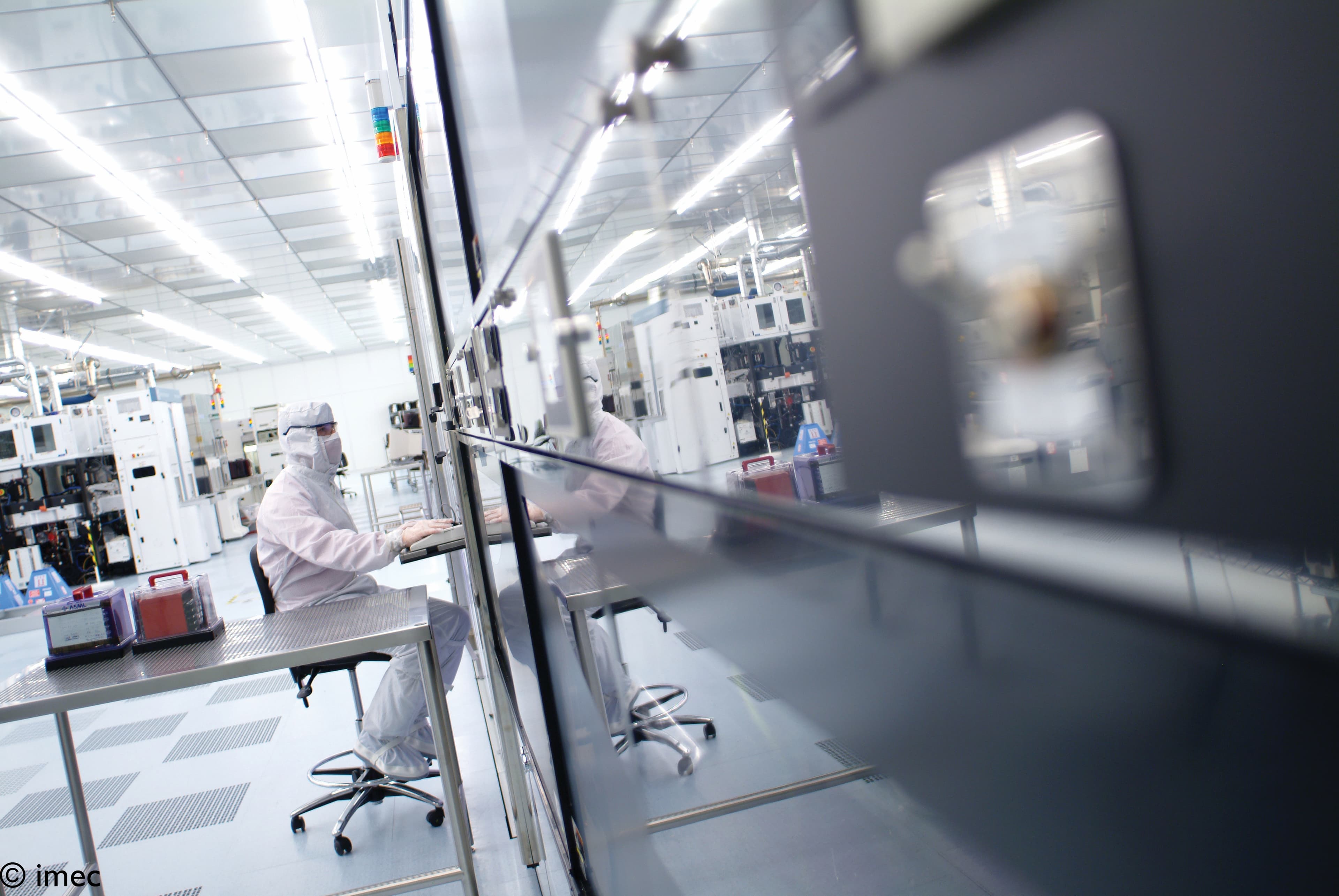
The beating heart of imec’s innovation activities is its 300mm cleanroom, the largest and most advanced R&D cleanroom in the world. For a quick tour, watch the video below:
Here, the world’s leading tool and material suppliers bring their instruments and technologies to create a unique, vendor-neutral lab where imec and its partners can explore new:
- patterning tools
- resist chemicals
- semiconductor materials
- analysis software
- semiconductor process technology tools
- process steps
Take a look at imec’s complete infrastructure.
The quality of imec’s infrastructure is matched by the excellence of its researchers, who continuously expand imec’s leading expertise in semiconductor technology domains such as patterning and process steps, metrology and characterization, reliability testing and modeling, and sustainable semiconductor technologies and systems.

Flexible collaboration models for semiconductor research and development
Do you come from industry – such as a foundry, IDM, fabless or fablite company, equipment or material supplier – or academia? Imec welcomes you to develop new processes for semiconductor technology, and to work out new products and ideas.
There are a number of ways to collaborate with imec:
1. Collaborative research
Enter one of imec’s research programs into next-generation semiconductor technology. You get privileged access to cutting-edge R&D results. And share costs and risks with other partners.
Imec hosts research programs in domains such as:
- Advanced logic scaling, going down to 1 nm and beyond through innovative device architectures, new materials and STCO.
- Storage and memory solutions, improving density, speed and energy-efficiency by exploring new concepts for technologies such as MRAM, DRAM, NAND and 3D Ferroelectric FETs (FeFETs).
- 3D processing and integration, boosting densities and bringing down costs through techniques such as die-to-wafer bonding and wafer-to-wafer stacking.
- Deeply scaled interconnects, approaching and surpassing the 3nm node through process innovations, scaling boosters and new materials.
- Optical interconnects, leveraging our silicon photonics platform to provide cost-efficient I/O solutions at all levels of computer systems.
- Neuromorphic circuits, using analog technology and in-memory computing to perform faster operations on large datasets.
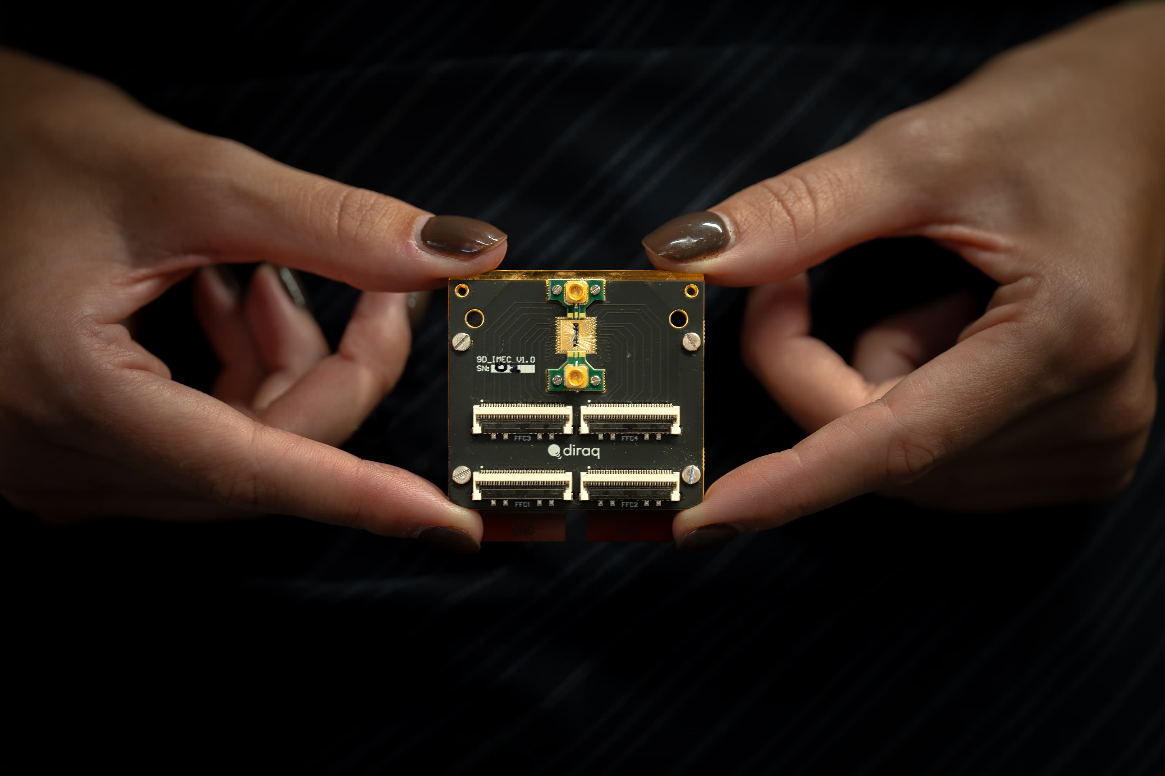
- Quantum computing, helping to overcome technological challenges, large-scale qubit fabrication, performance improvement and variability reduction of silicon and superconducting qubits, and 3D integration/packaging of cryocomponents.
- Sustainable semiconductor technologies and systems (SSTS), assessing and reducing the environmental footprint of IC technologies.
2. Bilateral research
Do you want an edge over your competitors when it comes to next-generation semiconductor technology? Then we’re happy to talk about an exclusive bilateral research collaboration.
3. Custom semiconductor R&D
Are you looking to enhance your product or service with an innovative component such as a microdevice? Then imec’s experts are ready to take on any challenge. That even involves prototyping, in-house low-volume manufacturing, and a path to high-volume manufacturing at one of our foundry partners.
4. Custom chip manufacturing
Are you ready to accelerate your path from concept to production?
Learn about IC-Link, imec's division for customized solutions for chip manufacturing.