
Sensing and actuation
Explore imec’s CMOS-based sensing and actuation innovations.
Sensor and actuator devices are multiplying in both consumer and professional domains. That’s in no small part due to the exceptional capability of semiconductor technology to downscale prices and form factors.
Imec aims to extend this path and enable new applications in domains such as life sciences and agrifood. We work on a wide array of sensor-actuator technologies – and their integration into comprehensive solutions.
Learn more about these technologies by clicking the images below. Or contact us directly for more information.

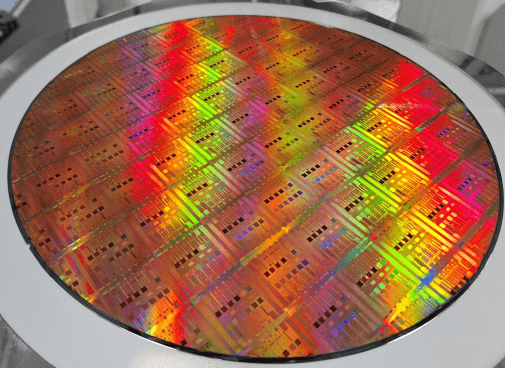
Optical sensing
Explore imec’s unique expertise in the development of CMOS- and photonics-based image sensors.

Ultrasound transducer technology
Take advantage of imec’s MEMS-based ultrasound transducer expertise and foundry-installed platform.

Radar and LiDAR sensing
Learn more about imec’s development of high-resolution and compact radar and LiDAR solutions.

Sensor data fusion
Learn more about imec’s data fusion solutions for diverse sensor types across a wide range of applications.

IoT sensors
Dive into innovative solutions for sensor networks, high-speed networks and sensor technologies.


What can we do for you?
- We offer flexible collaboration models ranging from pure contract research for concept design, prototyping and low volume manufacturing, to full support in process technology transfer and licensing to a CMOS foundry for high-volume production ramp-up.
- We offer custom product development with strong engagement model of collaboration matching your own internal R&D team objectives.
Why work with us?
- Our comprehensive expertise includes image processing expertise, HW and SW system design, calibration, simulation and more.
- Our unique CMOS semiconductor infrastructure includes a 1 billion euro state-of-the-art 200mm and 300mm cleanroom for process technology development.
- Ideal environment from early prototyping to ramping up small-volume production of up to 500 wafers per year per project.

Subscribe to our thematic newsletters