Pathfinding of emerging VLSI technologies and architectures with imperfect materials and processes
Leuven | More than two weeks ago
Safeguarding reliable operation of upcoming nanometer technologies
Our complete reliance on semiconductor technologies in all aspects of our lives guarantees their further enormous development in the foreseeable future. However, as device dimensions and spacing become smaller with every technology node, the devices themselves, including NanoSheets, ForkSheets and complementary FETs (CFETs), are also getting progressively more complex. Further abrupt shift is expected when 2D dichalcogenide channel FETs are transitioned to in 2030’s. Due to this ever-increasing complexity, the abundance of different scaling technology options for accentuating Power, Performance, Area- and Cost-effectiveness, and even environmental Sustainability, System/Technology Co-Optimization (STCO) has already become mainstream. However, it is still a daunting combinatorial task, often without a clear single optimal solution.
In this ongoing endeavor, VLSI materials development and processing need to keep up. More complicated geometries restrict available processing options, while the deposited layers are far from ideal. Atomic and microscopic defects, a reality in such highly thermodynamically unstable systems, will contribute to degradation with time (aging). Technologies based on materials, such as gate oxides, with excessive degradation for a given workload, will need to be pruned out of the pathfinding trees based on the Reliability criterion.
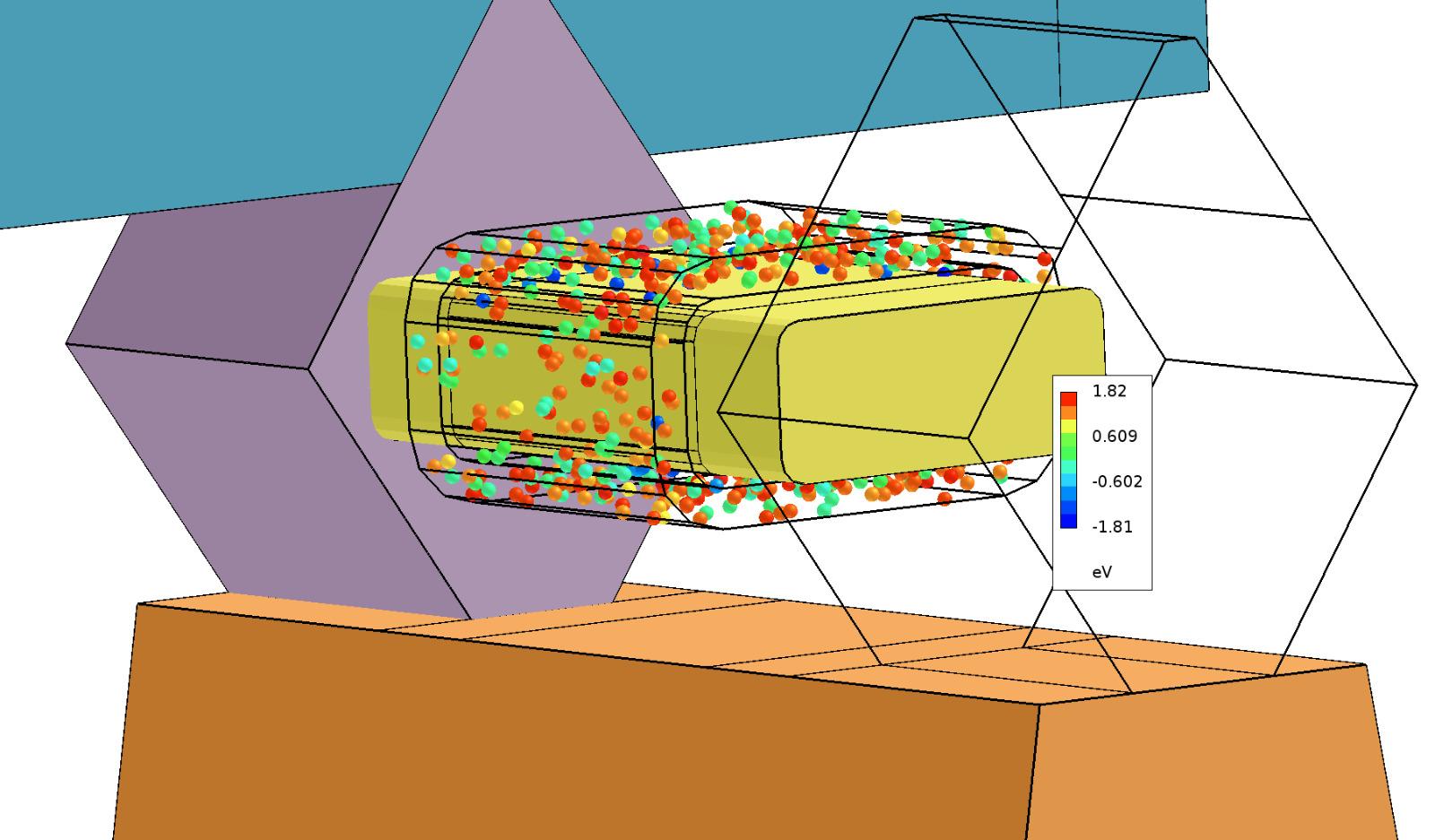
To classify the most vulnerable components in the emerging technologies in a systematic manner, previously developed Failure Mode and Effects Analysis (FMEA) methodologies can be applied. TCAD simulations of promising emerging architectures (individual devices and whole cells, such as SRAM) will be carried out with the vulnerable components having realistic defect densities. These reliability parameters, supplied by the reliability and processing teams, will allow simulating various degradation mechanisms, including Bias Temperature Instability, Hot Carrier Degradation, Time-Dependent Dielectric breakdown, Electromigration, Stress Induced Voiding and Self-Heating, for realistic workloads. In cooperation with the technology pathfinding team, this will help prioritize technologies and their aspects with respect to their reliability. Finally, a formal methodology should be developed for the multi-criterion optimization procedure including Reliability to down-select materials and architectures for emerging technologies.
https://ieeexplore.ieee.org/stamp/stamp.jsp?arnumber=9764470
https://ieeexplore.ieee.org/stamp/stamp.jsp?arnumber=6531974
https://ieeexplore.ieee.org/stamp/stamp.jsp?arnumber=9830450
https://ieeexplore.ieee.org/stamp/stamp.jsp?arnumber=9405172
https://ieeexplore.ieee.org/stamp/stamp.jsp?arnumber=9592527

Required background: TCAD, understanding of VLSI processing, circuit simulations, standard cells, and reliability fundamentals
Type of work: 80% modeling & simulation, 10% experimental, 10% literature
Supervisor: Bertrand Parvais
Daily advisor: Ben Kaczer
The reference code for this position is 2024-031. Mention this reference code on your application form.
