Sustainable Semiconductor Technologies and Systems (SSTS)
Imec’s Sustainable Semiconductor Technologies and Systems (SSTS) program sets out to assess, improve and disrupt fab processes to reduce their environmental impact.
Digital solutions can be used to address environmental and climate issues. Therefore, semiconductor technology is a vital ingredient for a more sustainable future. But what about our industry’s own environmental impact? Imec has estimated that IC manufacturing could account for 3% of total greenhouse gas emissions by 2040. That’s partly due to the growth of the industry. But it’s also linked to the fact that the process behind every new technology node becomes more complex and more energy-intensive.
And let’s not forget that the semiconductor industry’s ecological repercussions go beyond its contribution to climate change. They also include high water consumption, depletion of abiotic resources and generation of e-waste.
Download our white paper on the green transition of the IC industry

Semiconductor sustainability: from evaluation to improvement
For the semiconductor industry, limiting its environmental impact is more than a question of corporate responsibility. It’s also a matter of compliance with national and international guidelines, and – in the case of scarce materials – of business continuity.
No company can tackle this issue alone. It requires a collaborative effort by the complete ecosystem. The first priority is to close a glaring knowledge and data gap. Because quantification of the precise environmental impact of IC manufacturing of more advanced technologies, as well as its constituting elements, is severely lacking.
A correct assessment of this impact requires all industry players to agree on the methodological standards. And to openly share emissions in a standardized way. The next step is to use this data to devise improvements – both upstream of the fab and in the fab itself.
Imec is a central hub in the semiconductor ecosystem, with ties to practically all the industry players and experience in its own cleanrooms. This comes with access to a wealth of data. Through an established framework for design-technology co-optimization (DCTO), we can use this data and our research roadmap for the next-generation semiconductor nodes to take sustainability into account when making choices for future technologies.
Listen to the 3D InCites podcast where imec's Cédric Rolin talks about the SSTS program

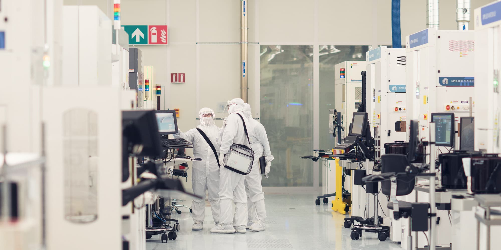
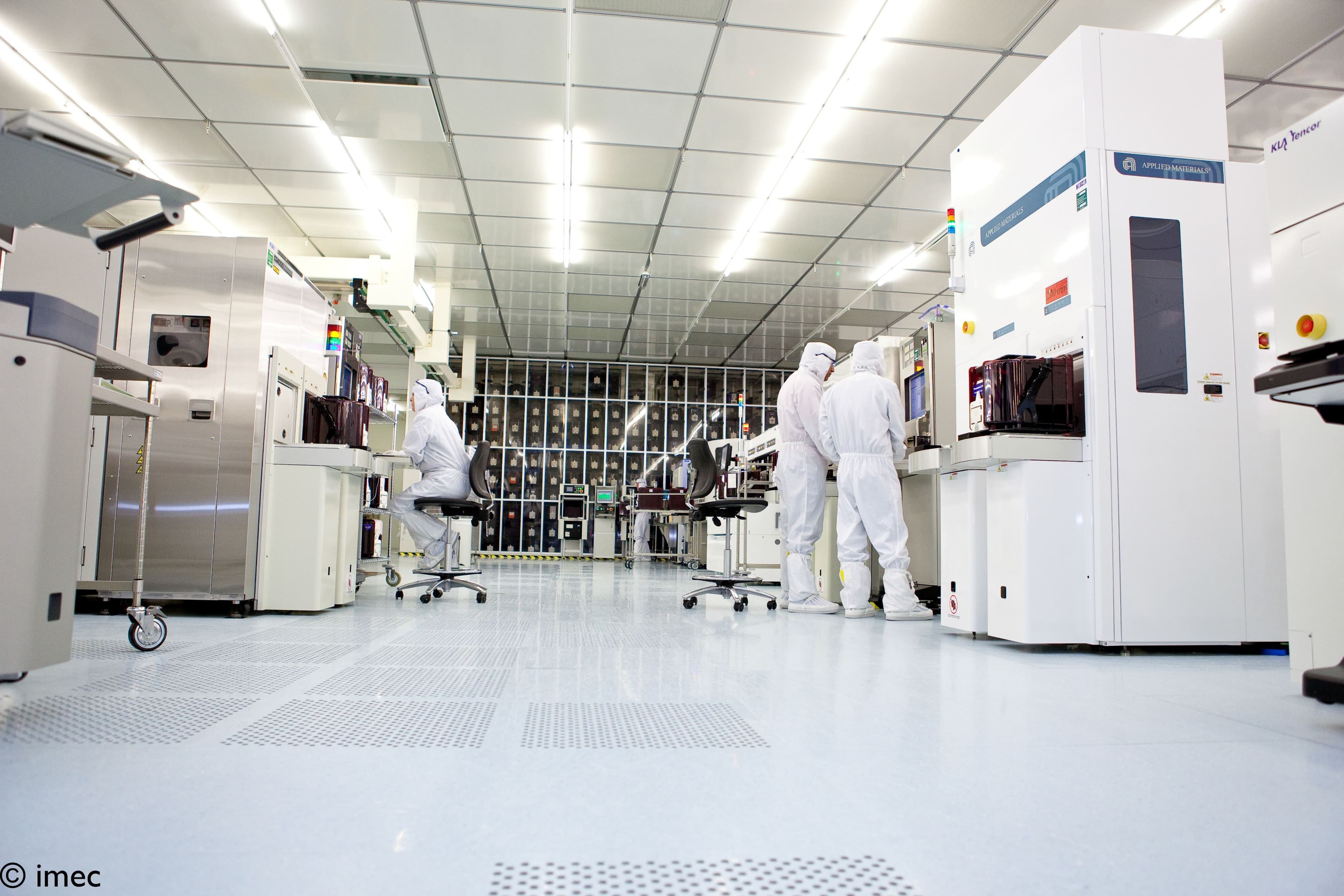
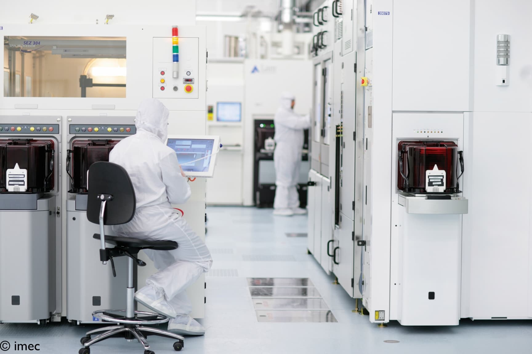
Imec’s advanced R&D fab is ideal for the assessment and mitigation of the environmental impact of semiconductor manufacturing.
Research pillars of the SSTS program: assess, improve, disrupt
To address the sustainability of the semiconductor industry, imec’s SSTS program combines in depth-fab modelling for impact assessment with research in the R&D fab for process improvement.
1. Assess – making a virtual fab
Using data from its own 300mm fab complemented with information coming from its ecosystem of material & equipment suppliers, imec is working on the consolidation of databases for process equipment, recipes, infrastructure, and libraries of process flows. Imec.netzero is a software platform that combines these datasets to reach a quantified, bottom-up understanding of the environmental impact of the manufacturing of semiconductor logic and memory technologies.
It makes precise estimations – for present and future IC technologies – of environmental impacts, such as:
- emission of process gases (such as NF3)
- energy consumption
- material usage
- water consumption
This virtual fab is constantly validated and enriched by benchmarking it against comparable manufacturing data from foundries and IDMs. This modelling effort supports:
- Closing data gaps in carbon accounting, as IC chips have a high climate change impact.
- Enabling pathfinding of the impact of future technologies and establishing decarbonation roadmaps.
- Providing a strong base for targeted and efficient R&D actions on the fab floor.

The imec.netzero tool is a software platform that combines datasets to reach a quantified, bottom-up understanding of the environmental impact of the manufacturing of semiconductor logic and memory technologies.
2. Improve with real solutions for the actual fab floor
Once imec.netzero has identified most of the high-impact problems, nothing’s in the way of tackling them with adjustments to current and future process flows. These can be evaluated with small-scale projects in imec’s fabs.
This step in particular requires ample input from material and equipment suppliers, as well as IDMs and foundries. To come up with ideas, and to evaluate them according to their relevance and feasibility for the industry.
Article: Validating sustainability strategies with real-fab solutions
As adjustments to current processes will not be sufficient to achieve the advances that are needed to keep semiconductor manufacturing on a sustainable path for the long term, we're also looking into revolutionary technologies that go beyond incremental improvements.
Want to join our research into semiconductor sustainability?
Imec’s SSTS program is looking for partners across the semiconductor value chain to share their expertise, from foundries, fabless and system companies, to IDMs and tool/material suppliers. Current program partners include Apple, Microsoft, ASM, ASML, KURITA, SCREEN, Tokyo Electron, GlobalFoundries, TSMC, Samsung Electronics, Air Liquide, AIST, Amazon, Applied Materials, Cadence, Central Glass, Edwards, Google, Intel, Intelligent Fluids, Lam Research, Merck, Meta, Micron, Nippon Sanso Holdings, Panasonic and Rapidus.
Membership provides you with access to SSTS results, and gives you a chance to help shape our roadmap. You will be at the forefront of one of the most important innovation domains in our industry, while minimizing your risks and expenses.