
Press release
Wood-based Biomass Resist Demonstrates Potential for Application in Cutting-Edge Semiconductor Processes
Ultrafine Pattern Formation Confirmed by High-NA EUV Lithography
Oji Holdings Corporation (Representative Director and President: Hiroyuki Isono, Headquarters: Tokyo) confirmed the successful formation of ultrafine patterns corresponding to the A14*1 process node with a wood-based biomass photoresist*2 (hereinafter referred to as “biomass resist”) for cutting-edge semiconductors in an evaluation using High-NA (numerical aperture 0.55) EUV lithography*3, a next-generation semiconductor manufacturing technology.
In recent years, with the rapid spread of AI, data centers, and high-performance computing (HPC), semiconductor devices are required to achieve even higher performance and lower power consumption. As circuit miniaturization continues to advance, High-NA EUV lithography is expected to be a core technology supporting next-generation semiconductor manufacturing.
In 2024, our company developed a biomass resist compatible with EUV lithography. Furthermore, with an eye toward commercialization, we began joint research with imec, one of the world’s leading research and innovation hubs in the semiconductor field, in 2025. This environmentally friendly next-generation photoresist is derived from wood-based biomass materials and delivers excellent ultrafine patterning performance while maintaining high storage and process stability, without the use of PFAS, which are subject to increasingly stringent regulations worldwide.
In this joint research with imec, we successfully demonstrated 10 nm-width line patterns and 16 nm-diameter hole patterns. These results confirm the applicability of our biomass resist to advanced semiconductor manufacturing processes and represent an important milestone toward its use in next-generation semiconductor technologies, including the A14 generation. We will continue to advance the material and process technologies to further improve performance.
This achievement is scheduled to be presented at “SPIE Photomask Technology + EUV Lithography 2026,” an international conference on semiconductor-related technologies to be held in Monterey, California, USA, from September 8 to 11, 2026.
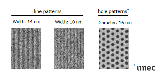
Pattern images from High-NA EUV lithography evaluation
* Successful etching was also achieved, confirming its potential applicability to manufacturing processes.
With the aim of commercialization in 2028, we will continue to improve the performance and accelerate the commercialization of biomass resists through joint research with imec and other research institutions, contributing to the advancement of the next-generation semiconductor industry and a more sustainable society.
- An indicator showing the manufacturing generation (miniaturization level) of semiconductors.
The A14 generation refers to the next-generation logic semiconductor node from 2028 onward
and requires technologies capable of supporting features of approximately 10 nm. Circuit pattern
miniaturization enables higher performance, lower power consumption, and greater integration
of semiconductors. - A photosensitive material used to form circuit patterns in the semiconductor manufacturing
process. - A next-generation lithography technology for forming semiconductor circuits using extremely
short-wavelength light called extreme ultraviolet (EUV). It achieves higher resolution than
conventional NA (numerical aperture 0.33) EUV lithography, enabling the formation of finer
patterns. It is expected to support the development of higher-performance next-generation
semiconductors.