Charge trapping in advanced CMOS devices at cryogenic temperatures for quantum computing applications
Leuven | More than two weeks ago
Unravel fundamental reliability physics to enable large-scale quantum computing
Quantum computing emerges rapidly as a research field that has the potential to bring to practice technologies exploiting massive parallelism and to push computational power way beyond the contemporary realm for a certain class of problems. Because of fundamental limits to the tolerable operating temperature of some of the leading candidate-qubits, one major hurdle towards large-scale integration is their interface to the classical control circuitry required to operate them.
A promising approach to overcome this problem is to deploy traditional CMOS circuitry in cryogenic environments for efficient operation of future quantum computers by reducing limitations due to wiring and signal integrity.
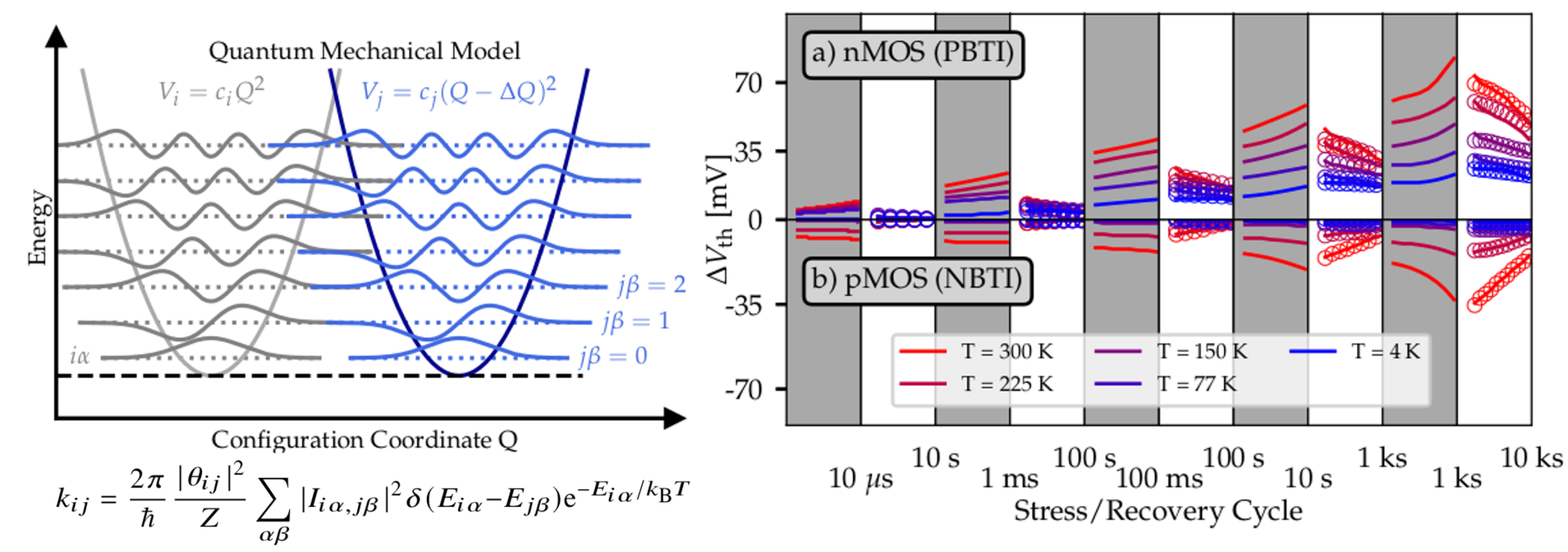
Traditional reliability models like random telegraph noise, bias temperature instability, and hot-carrier degradation are thought to freeze out at low temperatures. However, recent experimental studies have reported an unexpected weakening of the temperature dependence of charge trapping phenomena at cryogenic temperatures, suggesting the need for a fundamental revision and expansion of common degradation models.
What you will do:
- You will measure the electrical impact of defect generation and charge trapping in advanced CMOS devices from room-temperature down to cryogenic temperatures.
- You will design and execute specific experiments to unravel fundamental defect physics of cryo-CMOS stacks independently of the underlying technology.
- Your studies will help to explore the limits of traditional reliability models and improve our understanding of defects in MOS devices at cryogenic temperatures.
- You will identify the key parameters and expand the modelling of defects and device-to-device variations on the operation of advanced CMOS devices at deep cryogenic temperatures.
Who you are:
- You have a master’s degree in electrical engineering, microelectronics, computational physics, or related fields.
- You would like to understand and model the physics of defects in MOS stacks at cryogenic temperatures on a fundamental level.
- You want to gain hands-on measurement experience in our cryo-lab.
- You like to take the initiative; you are persuasive and assured, while keeping a constructive attitude within the team.
- Given the international character of imec, a fluent knowledge of English is necessary.
Figure 1: Left: Quantum mechanical formulation of the non-radiative multi phonon model to explain oxide defect kinetics at 4K. Right: Simulation results vs. measurement data for threshold voltage drift as function of temperature and stress time.
Required background: electrical engineering, microelectronics, computational physics, or related fields
Type of work: 40% electrical characterization of CMOS devices at various temperatures, 40% data analysis and modeling, 20% literature research
Supervisor: Valeri Afanasiev
Co-supervisor: Stanislav Tyaginov
Daily advisor: Alexander Grill
The reference code for this position is 2024-043. Mention this reference code on your application form.