Design of Nanostructured Arrays for Ultrafast Surface-Enhanced Spectroscopies of EUV Photoresists
Master projects/internships - Leuven | More than two weeks ago
Design, build (using compatible CMOS fabrication processes), and possibly (time-allowing) test nanoengineered substrates for plasmonic enhanced spectroscopic signals in sub-picosecond time-resolved near-to-mid IR absorption spectroscopies of current and next-gen EUV photoresists.
Current state-of-the-art lithography tools employ extreme ultraviolet (EUV) light to expose photoresists for creating the nanoscale features that form the building blocks of today’s (and tomorrow’s) microelectronics. While EUV lithography is currently being used in high-volume manufacturing, the chemical transformation of the photoresist during EUV exposure is still not completely understood. This hinders the advancement and controlled engineering of resist formulations to optimize their performance to print smaller features (and thus faster and denser circuits).
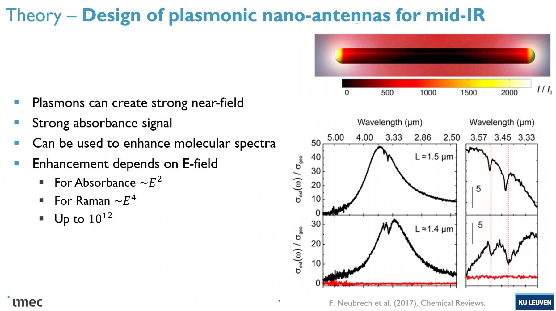
Time-resolved spectroscopies (using EUV pulses as a pump and near-to-mid infrared (IR) pulses as a probe) are currently being developed within imec’s AttoLab to track chemical changes in the photoresist in real time, during the EUV exposure. However, the IR absorption signals from thin-film photoresists (typically, 10’s of nanometers) are quite low, thus preventing the detection of trace and/or transient chemical species. To increase these faint transient signals, we aim to use nanostructured arrays with near-to-mid IR localized surface plasmon resonances (LSPRs) that can enhance the probing IR beam.
This position supports this goal by computational modelling of engineered nanostructures and optimization of their composition, geometry (size/shape), and surrounding environment to yield the strongest LSPR in the near-to-mid IR spectrum. In particular, the student will design the nanostructured arrays and simulate their near-field optical properties following excitation by near-to-mid IR femtosecond pulses. Optimization of the target structures will be performed using finite-difference time-domain electromagnetic simulations and optimized structures and geometries will be scrutinized for FAB-based production. The student will work closely with the AttoLab science team as well as with a diverse set of technical experts in lithography, plasmonics, optics, lasers, and time-resolved spectroscopies. As such, this multidisciplinary project provides a venue to enhance knowledge in nanoplasmonics as well introduce the student to concepts of lithographic manufacturing and laser-based spectroscopy.
Type of Project: Combination of internship and thesis; Internship
Master's degree: Master of Science
Duration: 1 year
Master program: Nanoscience & Nanotechnology; Physics; Chemistry/Chemical Engineering
Supervisor: Pol Van Dorpe
Supervising scientist(s): For further information or for application, please contact John Petersen (john.petersen@imec.be) and Fabian Holzmeier (fabian.holzmeier@imec.be)
Only for self-supporting students