Experimental Characterization of Mid-Infrared GeSi Integrated Photonics
Master projects/internships - Leuven | More than two weeks ago
Exploring GeSi integrated photonics platform for mid-IR sensing
Germanium has emerged as a key enabler for mid-infrared (mid-IR) integrated photonics thanks to its exceptional broad optical transparency window from 1.9 to 16.7 μm, unlocking critical chemical sensing and spectroscopy applications in mid-IR range. Combined with the inherent CMOS compatibility, Ge-on-Si platforms enable scalable, cost-effective integration of mid-IR photonic circuits with Silicon electronic systems, paving the way for compact, high-performance solutions in mid-IR sensing, imaging, and communications.
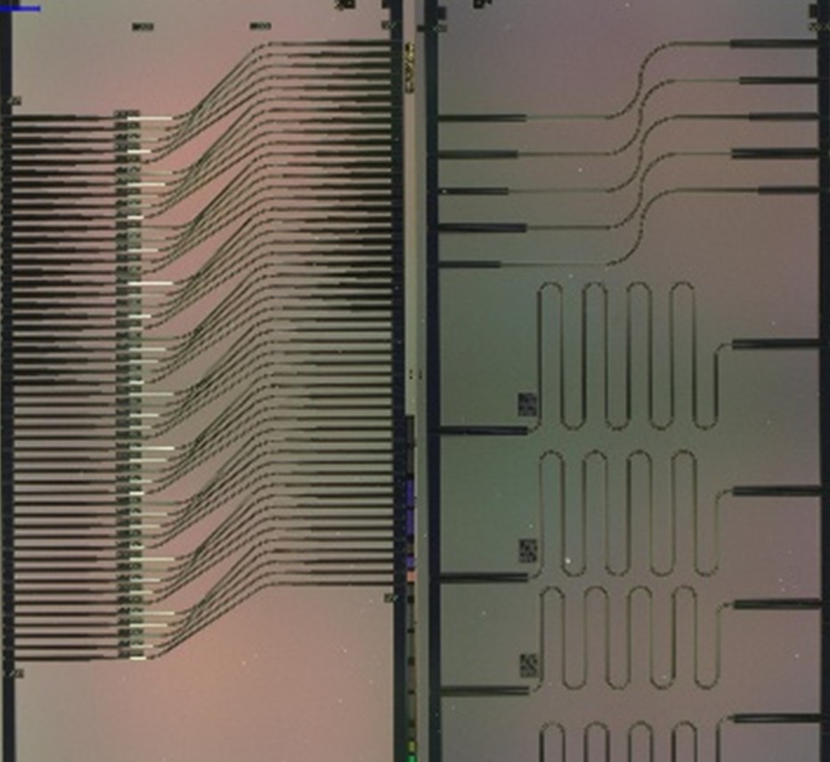
At imec, we are developing mid-IR integrated photonics through the development of germanium–silicon (GeSi) wafers tailored for advanced sensing applications. Our initial fabrication run has produced wafers with essential photonic building blocks (right plot), e.g., edge couplers, waveguide spirals, and ring resonators, alongside test structures for assessing coupling efficiency, propagation loss, and platform performance. To support this effort, we have established a free-space optical test bench featuring a tunable mid-IR laser source (8–11 µm), alignment stages, and lock-in IR detection for high-sensitivity measurements.
In this project, we are looking for a master’s student to take an active role in:
- Optimizing free-space optical measurement setups
- Characterizing GeSi photonic components
- Quantifying coupling efficiency, propagation loss, and resonator performance
- Interpreting results to inform the next design and fabrication cycle in close collaboration with imec’s multidisciplinary teams
What will you learn:
- Hands-on experience in mid-IR photonic device testing and imaging
- Data acquisition, signal processing, instrumentation, and experimental troubleshooting
- Understanding of GeSi material properties and integrated photonics for sensing, communications, and spectroscopy
Who are we looking for:
- Master’s student in photonics, optics, applied physics, electrical engineering, or a related field
- Strong interest in experimental work, optical measurements, and photonic devices
- Motivation, curiosity, and comfort working in a laboratory environment
Why join us:
You will work on an emerging mid-IR platform with potential for next-generation sensing and integrated photonic systems. This internship offers the chance to influence real hardware development and gain hands-on expertise in a rapidly expanding domain.
Type of Internship: Master internship
Master's degree: Master of Engineering Technology; Master of Science
Duration: 6 Months, to be determined with student.
Required educational background: Nanoscience & Nanotechnology; Electromechanical engineering; Materials Engineering
University Promotor: Pol Van Dorpe (Physics, Nano)
For more information or application, please contact the supervising scientist Liwang Liu (liwang.liu@imec.be). Please include your resume and a brief motivation statement in your mail.
Imec allowance will be provided.