[NanoIC topic] Scaled source/drain epitaxial layers for nanosheet & complementary field-effect transistors
PhD - Leuven | More than two weeks ago
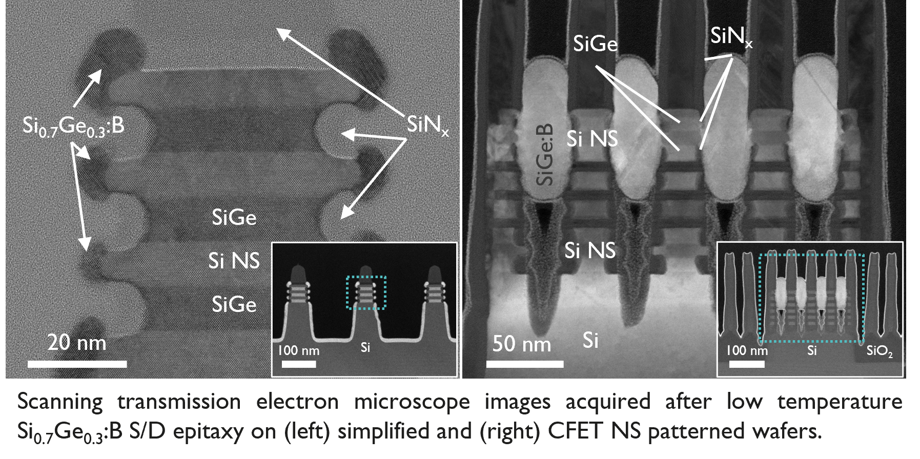
The complementary field-effect transistor (CFET), based on stacked nanosheet (NS) devices, is the main candidate for CMOS technologies beyond the 1 nm node. In such devices, highly doped SiGe:B and Si:P epitaxial layers are used as p- and n-type source/drain (S/D) terminals, respectively. These materials need to grow in high aspect ratio cavities, from scaled Si open areas surrounded by dielectrics (e.g. SiNx), and from surfaces exhibiting different crystal orientations, in comparison to previous device generations. However, reactions determining growth and doping activation mechanisms, and hence the resulting contact properties, are not well understood. The objective of the PhD therefore is to gain fundamental insights into the physical mechanisms governing the S/D formation, on how these properties are affected by specific device architectures, and how this links with the resulting contact and device properties. The PhD candidate will acquire hands-in epitaxial growth and material characterization experience using state-of-the-art 300 mm industry-compatible tools. The epitaxial growth studies will be supported by first-principles simulations to underpin process fundamentals. The PhD will take place within the imec epitaxy team at imec headquarters, Leuven, Belgium, in collaboration with KU Leuven. The candidate will benefit from multidisciplinary expertise within a highly international environment conducive to innovation.
Required background: Physics, Material science
Type of work: 70% experimental, 30% modeling/simulation
Supervisor: Claudia Fleischmann
Co-supervisor: Clement Porret
Daily advisor: Thomas Dursap
The reference code for this position is 2026-012. Mention this reference code on your application form.