Bringing chip patterns onto a wafer: the conventional way of working
Manufacturing chips for advanced logic applications starts with designing the electrical circuit. This process happens at different levels: from transistors over standard cells and place-and-route, up to the system design level. The patterns forming the circuit design layout are then written onto a photomask. Today, this is done by mask writing tools that make use of electron beams, such as the variable shaped beam (VSB) mask writer and multi-beam mask writer (MBMW). Next, in a photolithography exposure step, the pattern on the mask is downsized and projected onto the photoresist layer on top of the target wafer. After the resist development, the printed pattern is further transferred into the underlying layers of the substrate using advanced patterning and etch techniques.
During the photolithography exposure step, the intended circuit layout image gets distorted. This is due to the way light propagates through the lithography scanner and mask, undergoing diffraction. The distortion translates into poor image fidelity, which is the difference between the target image and the printed structure on the wafer. The latter appears with irregularities such as line widths that are narrower or wider than designed, compromising edge placement integrity and resolution. Optical proximity correction (OPC) techniques are, therefore, applied to the layout design data: they correct the pattern before it is written on the mask to minimize errors from design to wafer.
Advancements in photolithography, mask, and OPC technology have been pivotal in driving the power-performance-area-cost (PPAC) improvements of subsequent logic technology generations. Resolution enhancements have been achieved by reducing the wavelength of the light used for the exposure step or by increasing the numerical aperture (NA) of the lithography scanner. Examples of the latter are the evolution from 193nm to 193nm immersion lithography, extreme ultraviolet lithography (EUV) and the forthcoming move to 0.55NA extreme ultraviolet lithography (High NA EUV).
The design side also evolved to keep pace with the resolution enhancement offered by improved photolithography techniques. The pitch scaling demanded by successive technology nodes outpaced the advancements in photolithography. When that happened, designs for advanced logic chips moved away from 2-D Manhattan- to 1-D Manhattan-based circuit layouts in the critical layers. In 2-D Manhattan-based designs, rectangular structures are used to align along both vertical and horizontal directions. In contrast, 1-D designs in the critical layers align structures to either vertical or horizontal directions per layer. Although 1-D Manhattan offers a dense representation, it comes with a downside: when making an electrical connection from one metal line to a neighboring one, an extra layer with a number of vias has to be implemented – adding to the wafer cost, and the path length of the electrical current.
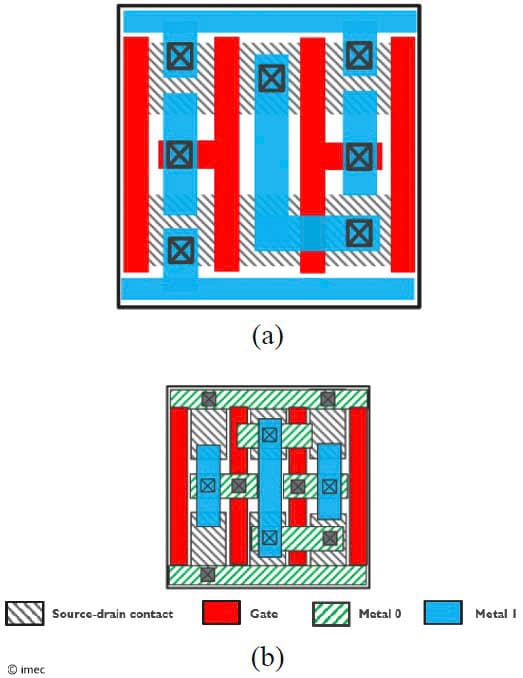
Figure 1 – Schematic illustration of (a) a 2-D Manhattan-based standard cell design for technology node N and (b) 1-D standard cell design for technology node N+1, requiring an extra M0 layer for intracell routing.
Do you want regular updates on imec’s semiconductor research?
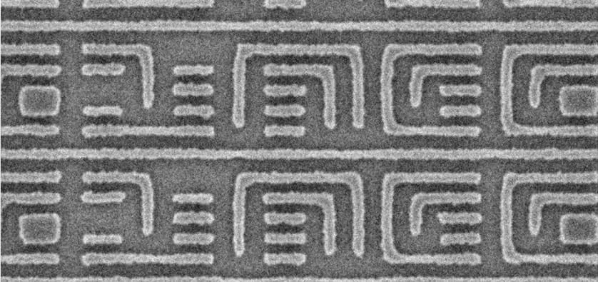
In all this, there is one ‘peculiarity’: although designers today pursue rectangular, Manhattan-shaped structures in their design, the structures always appear as curved on both mask and wafer. This is an inherent consequence of how the mask writer and lithography scanner operate, acting as a low-pass filter for electron beams and light, respectively. Manhattan designs, therefore, become curved when transferred through the system, inducing additional errors in the final patterns.
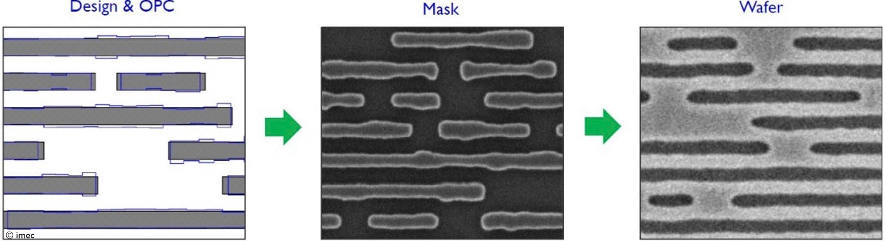
Figure 2 – Manhattan designs become curved when transferred through the lithography system.
Introducing ‘curvilinear’ in OPC and masks: reducing errors and improving the process window
A few years ago, the lithography community started exploring the idea of introducing curvilinear shapes when writing circuit patterns onto the photomask. This was facilitated by the emergence of the multi-e-beam mask writing tool, which, for the first time, enabled complicated shapes to be written on the mask. This assists in further minimizing the errors that occur along the path from Manhattan-based designs to curvilinear representations on the wafer.
More recently, the community also considered using new OPC algorithms that adjust the Manhattan design layouts towards the more complex curvilinear shapes on mask and wafer. Novel ‘curvilinear’ OPC techniques in conventional OPC and inverse lithography technology (ILT) started to emerge as a way to improve the process window of the photolithography step.
Both curvilinear mask and OPC techniques have recently become hot R&D topics in the semiconductor industry, which is reflected by the growing number of contributions at the 2025 SPIE Advanced Lithography and Patterning Conference.
Introducing curvilinear in the design space: node-to-node transitions at reduced wafer cost
Curvilinear OPC and mask strategies both still start from Manhattan circuit design layouts. As a next step, imec proposes to introduce curvilinear geometries and paths already in the design phase, an innovative concept with far greater benefits than curvilinear OPC and mask strategies. Opposed to current roadmap evolutions, curvilinear design promises to enable technology node transitions at reduced wafer manufacturing cost while improving electrical performance [1-2]. It is, therefore, believed to transform the semiconductor industry, as shown by imec in an invited paper at the 2025 SPIE Advanced Lithography and Patterning Conference[3]. The benefits are demonstrated with three use cases.
Use case 1: simplifying middle-of-line (MOL) and backend-of-line (BEOL) layers and vias through curvilinear design
A first use case where curvilinear design proves beneficial is a routing exercise for standard cell and place-and-route designs for metal layers of tight pitch.
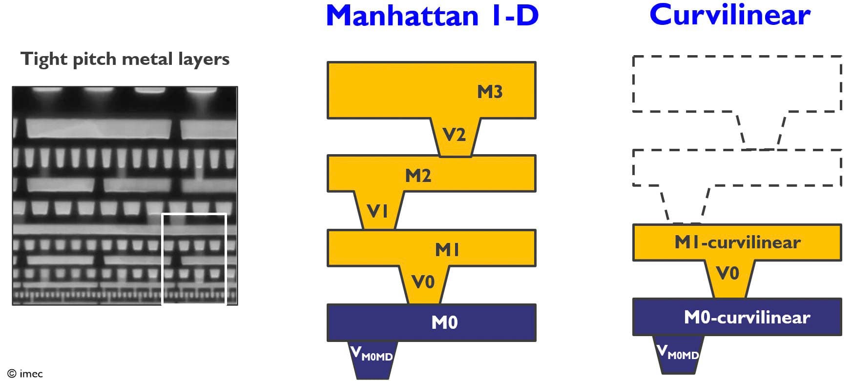
Figure 3 – Eliminating expensive metal and via layers by using curvilinear designs.
For foundry 14A and beyond, adopting curvilinear designs in standard cells and tight-pitch metal layers allows combining the most expensive MOL and BEOL layers to reduce the number of metal layers required, thereby also eliminating corresponding vias. Emulations show that a 7% wafer cost reduction, a 5% shorter fab turn-around time and 7% fewer process steps are achieved if the curvilinear design can successfully eliminate M2 and V1 – one metal layer. Imec researchers also assessed the impact on electrical performance for this particular use case: the curvilinear design exhibits about 5% performance improvement compared to a Manhattan 1-D design at the standard cell level. The metric for improvement is the reduced delay time, which results from the absence of the extra via and the shorter metal path for the electrical current.
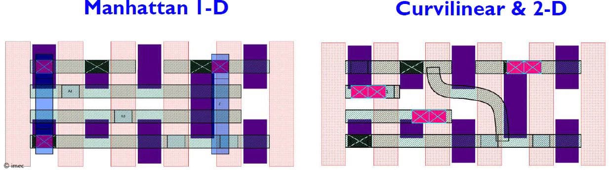
Figure 4 – (Left) Manhattan 1-D and (right) curvilinear standard cell layout for industry 14A technology node.
Use case 2: source/drain contact and gate re-routing through curvilinear design
A second opportunity for using curvilinear designs is in the routing between the source/drain contacts and gates of the n- and p-type transistors that make up the CMOS device. With today’s 1-D Manhattan design, they can form an electrical connection only ‘north-south.’ Hence, the only way to connect the source/drains and gate of n- and p-type transistors is by adding an extra metal and via layer. This allows the electrical current to go up through the via, run along the routing metal in the extra layer, and come down through another via to connect to the other source/drain contact. Hence, electrical and cost penalties are incurred.
However, using a curvilinear shape to connect the source/drain contacts and gates allows to eliminate the electrical connections using extra metal layers. Reducing the M0 routing resource utilization allows for further cell area scaling. Applying this concept to a logic standard cell of an industry foundry 14A node shows a 20% reduction of the area (corresponding to a transition from 5T cell design to 4T cell design) while suppressing wafer manufacturing costs.
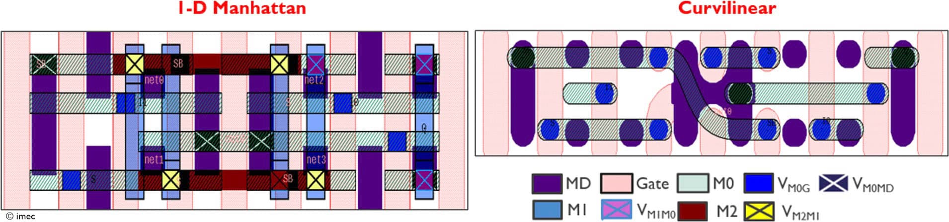
Figure 5 – Source/drain contact and gate routing using (left) 1-D Manhattan and (right) curvilinear designs. Curvilinear design completes the design within M0 while Manhattan design requires M2.
Use case 3: curvilinear place-and-route design
Compared to use cases 1 and 2, imec identifies the greatest potential for curvilinear geometry at the place-and-route level, where its application extends across all metal routing layers above the standard cells. Unlike the previously described use cases, this approach demands a significantly greater industrial effort, including fully enabling place-and-route tools and parasitic extraction EDA solutions across the entire design space. By achieving this, imec anticipates that curvilinear technology will play a key role in extending logic technology nodes into the future.
The overall benefits of using curvilinear designs can be demonstrated by using power-performance-area-cost (PPAC) figure-of-merits. Today, while specific targets vary, a representative example of node-to-node transition goals includes a 20% reduction in area, a 15% improvement in performance, and a 15% improvement in power consumption. These PPA benefits today come with a trade-off in wafer manufacturing costs: the industry tries to limit this cost increase to 20% node-to-node. By adding curvilinear shapes in the design layout, an additional area reduction in combination with power/performance improvement can be obtained compared to using 14A Manhattan 1-D designs – following an estimation by imec. This means that the industry may progress into 10A without scaling the dimensions (i.e. pitches). More importantly, these benefits come with a cost reduction. It is an excellent example of how design-technology co-optimization (DTCO) in the field of patterning can further enhance the PPAC benefits of node-to-node transitions.
From curvilinear design to wafer printing: a manufacturable solution
Imec is the first to provide a solution for enabling curvilinear data representations in the chip’s design phase. In addition, the research team developed a comprehensive flow that is manufacturable through the stages of OPC, mask, and wafer printing. These breakthroughs are the result of building a full ecosystem with EDA vendors, mask manufacturers, and chip manufacturers – a continuing effort that started in 2023.
Curvilinear data generation while keeping data volume under control
Establishing curvilinear designs is challenging for several reasons. Until now, no solution has been found to enable accurate data representations of curvilinear shapes while keeping the data volume under control across the manufacturing ecosystem. One option is to approximate the curved shapes using a piece-wise rectilinear data representation, a geometric configuration composed of straight lines in connecting points. However, using this representation would increase the data volume tremendously. Excessive data volume is a concern for the industry, as commercial EDA tools struggle to handle these large volumes, and data must also be transferred across the manufacturing ecosystem.
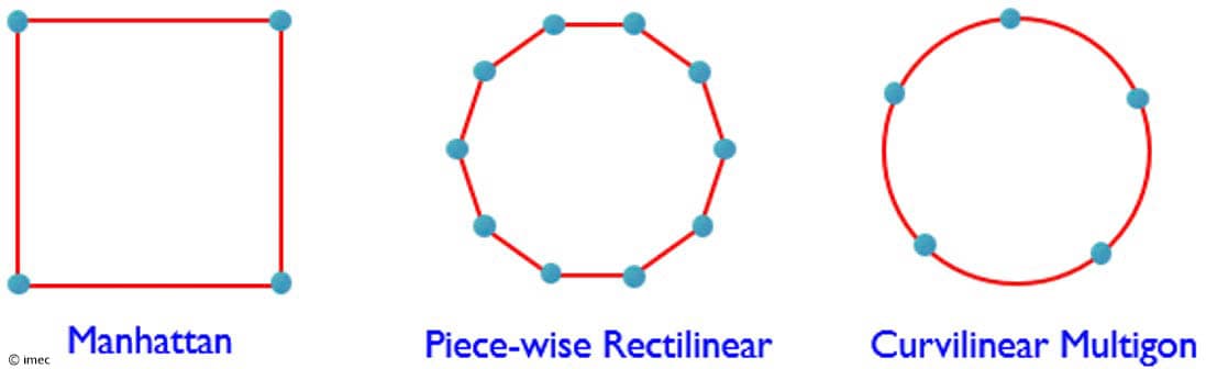
Figure 6 - Classification of shapes.
Also, dedicated design rules that contain information about the device components and layout features need to be established. In addition, a method must be found to verify that the design is correct – the so-called design rule check (DRC). And all this must be manageable by commercial EDA tools.
Imec has developed a way to generate curvilinear data while keeping the data volume under control: using so-called parametric curve generation (such as Bezier and BSpline) for a limited number of features that offer the largest benefits when curvilinear. The remaining features can be represented using the traditional data representations used for Manhattan designs to suppress the data volume increase. This ‘two-stage’ approach was also used for validating design rules: traditional Manhattan DRC is applied to Manhattan features, while specific curvilinear DRC is used on a limited set of curvilinear design data.
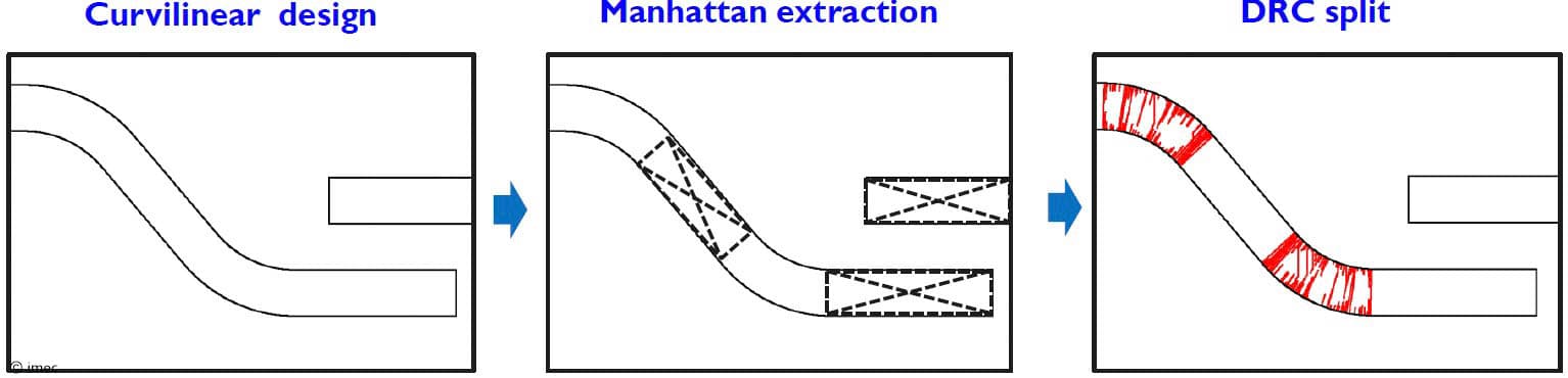
Figure 7 – Two-stage DRC verification: (left) use curvilinear design only where necessary; (middle) apply Manhattan DRC on the Manhattan shapes; and (right) use curvilinear point-to-point DRC to curvilinear segments only.
Strategies for curvilinear OPC, mask, and wafer
Imec also developed strategies for curvilinear OPC and mask, leveraging earlier developments in curvilinear OPC and multi-e-beam mask writing. The curvilinear OPC serves as a critical step in realizing the printed wafer image as close as possible to the curvilinear design intent. Imec, together with its partners in EDA, made substantial progress in providing commercial CurviOPC EDA tools. They are also developing simplified mask rules and verification strategies, affordable for manufacturing.
At the wafer level, imec has demonstrated printability of the curvilinear ‘use cases’ on full 300mm wafers.
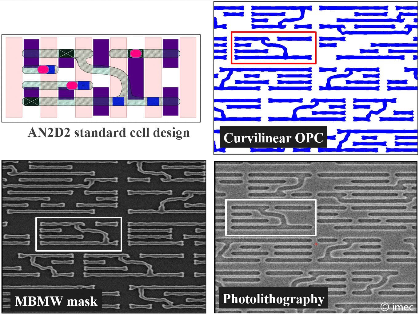
Figure 8 – From curvilinear design over OPC to mask to wafer-level printing.
Outlook: validation at the system level; expanding the use cases; call for collaboration
The imec researchers have shown the merits of utilizing curvilinear design, particularly in terms of enhancing electrical performance and reducing manufacturing costs when transitioning from one advanced logic node to the next. The advantages have so far been shown at the standard cell level and for limited place-and-route. In future work, the team will expand the PPAC assessment to the chip level to further prove its usefulness.
In addition, a comprehensive workflow has been established that facilitates the integration of curvilinear design across the semiconductor ecosystem, from the design phase to wafer manufacturing. Imec calls upon EDA houses, computational lithography experts, mask manufacturers, and collaborating partners to intensify ecosystem collaborations, benefiting the entire semiconductor industry.
Imec also demonstrated the compatibility of using curvilinearly designed shapes with High NA EUV lithography, the next leap in photolithography. Because of the benefits mentioned above, the curvilinear design concept promises to make more efficient use of High NA EUV lithography – making it a complementary technology option for advanced logic nodes. But the novel concept is also expected to extend low NA EUV lithography, particularly 193nm immersion lithography, which is relevant in other application areas such as image sensors, meta lenses or automotive chips, which can benefit from the reduced manufacturing costs.
This article was originally published in Semiconductor Digest.
Want to know more?
[1] “Curvilinear standard cell design for semiconductor manufacturing”, R.-H. Kim et al.,IEEE Transactions on Semiconductor Manufacturing, vol. 37, no. 2, pp. 152-159, May 2024, doi: 10.1109/TSM.2024.3362900.
[2]"Manufacturing-friendly curvilinear standard cell design", R.-H. Kim et al., Proc. SPIE 12954, DTCO and Computational Patterning III, 1295405 (April 2024); https://doi.org/10.1117/12.3009888
[3] “Integration of curvilinear design into semiconductor logic technology and its manufacturability”, R.-H. Kim et al., Invited paper at the 2025 SPIE Advanced Lithography and Patterning conference.