Nanoimprint lithography
Realize high-resolution patterning with attractive cost of ownership with imec’s nanoimprint lithography (NIL) offering – uniquely embedded in our advanced lithography fab ecosystem.
Nanoimprint lithography enables the replication of sub-micrometric features at wafer level and on any substrates. It’s been around for quite some time. And yet, we’ve barely scratched the surface of its many possibilities. The process is used for production purposes, but mostly in a semi-automated fashion and mainly not in a semiconductor fabrication process flow.
To unleash the full potential of nanoimprint lithography, it’s time to mature the technology towards an automated, reliable foundry process that allows its integration in semiconductor manufacturing.

Scanning Electron Micrograph (SEM) of wafer cross-section.
This maturation of nanoimprint lithography is imec’s goal. By leveraging its process capabilities for all the steps before and after imprinting, such as optical design, master manufacturing, etching and metrology, imec offers its industrial partners access to process development and low-volume manufacturing of NIL-printed devices for applications such as augmented reality and genomics.
A full NIL portfolio under one roof
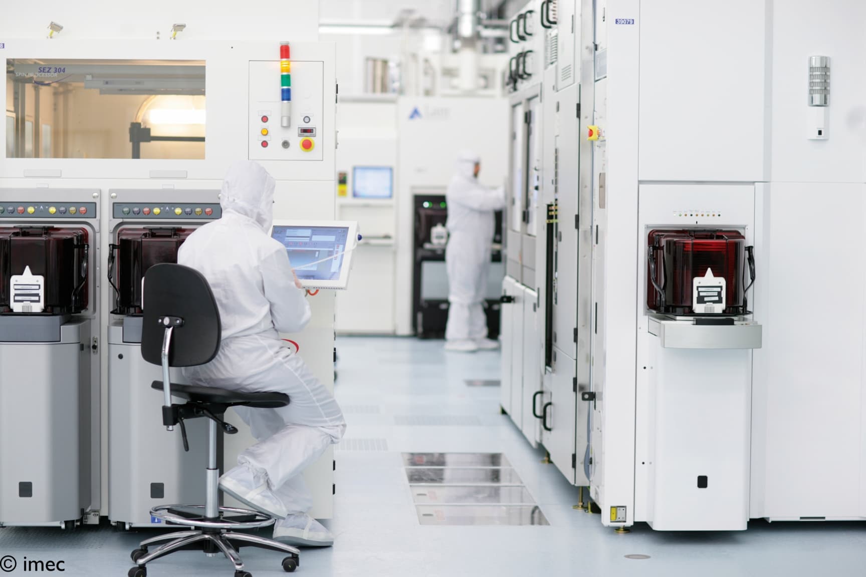
At the heart of imec’s NIL offering is its fully automated 200- and 300mm platform with integrated modules for manufacturing working stamps, wafer cleaning and etching, imprinting, and post-imprint thermal curing.
But it takes more than one tool to achieve a successful NIL process. That’s why we offer support for all the steps of the workflow:
Technology-aware master manufacturing
- master layout definition by our optical design teams
- manufacturing of large-area high-resolution masters by our fab teams in the 200- and 300mm cleanrooms
Process development
- screening and validation of materials by our technology teams in collaboration with our extensive network of resin suppliers
- custom development of a 200- or 300mm imprint process
- integration of imprinted optical elements on top of CMOS
- process screening and low-volume manufacturing
By integrating nanoimprint lithography in a semiconductor manufacturing environment, we can support the development of production processes for a wide range of disruptive applications.

Scanning Electron Micrograph of patterns imprinted from the stamp into a NIL resin. On the left: field of densely packed nanowells, diameter of 350 nm, height of 150 nm and resin residual layer at the bottom of the well of less than 20 nm. On the right: field of periodic gratings, width of 200 nm, pitch of 400 nm, height of 150 nm. Residual layer between the lines of less than 20 nm.
Nanoimprint lithography applications
A lot of applications can benefit from the integration of nanoimprint lithography in their production process. A few examples:
- genomics/DNA sequencing – On-chip analysis tools demand high-density nanopatterning, compatibility with glass substrates, and resilience to harsh chemical environments.
- augmented reality – The production of its displays needs high fidelity over large areas, precise tuning of optical properties, and flawless grating smoothness.
- consumer electronics – Camera components benefit from high-volume, large-area and wafer-level micro-lens manufacturing that can be aligned to substrate features such as pre-patterned apertures.
- automotive technology – The gradual automation of the driving experience is leading to a constant increase of sensing devices on most vehicles, to allow features such as adaptive cruise control, environment mapping and smart illumination. These are often based on optical gratings and micro-optics to be manufactured on a large scale via NIL.
Are you interested in working with us on these or other applications? We’re ready to support you through all the development phases: from feasibility study and design up to prototyping and low-volume manufacturing.