Application of Continual Machine Learning and Causal Inference in Semiconductor Process Optimization: Towards Artificial General Intelligence
Leuven | More than two weeks ago
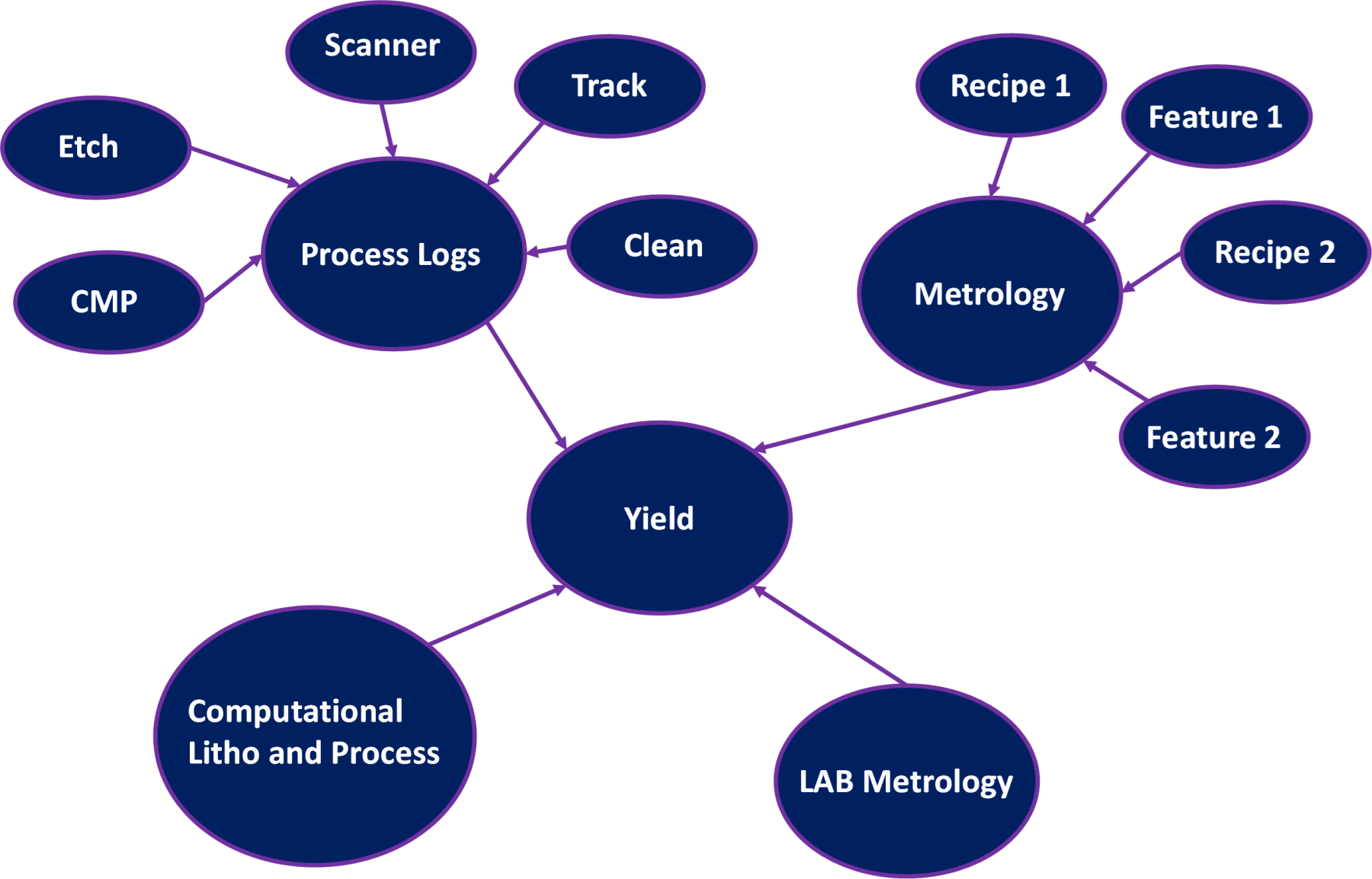
The goal of this research is to investigate continual learning adaptability in semiconductor process optimization and to establish the causal relationships (causal inference) in a data-centric approach.
The PhD student accepted for this position will learn conventional process flow and will be responsible to work collaboratively toward developing and applying “Machine learning" based optimization algorithms with a goal to tackle the aforementioned challenges in terms of 1) Reducing computational cost, 2) reduce tool cycle time, 3) predictive process control approach in enabling advanced node semiconductor manufacturing. 4) Improving metrology data.
Machine learning applicability includes:
- Brainstorm “Technical diligence” of the project: to meet desired performance and engineering timeline.
- Tool Data Analysis: Collect data, analyse data, and suggest hypothesis with expert feedback loop.
- To understand and establish the causal relationships (causal inference) in a data-centric approach.
- To investigate continual learning adaptability and applications in semiconductor process optimization.
- Image Processing applicability: Collect Image data (SEM/TEM/EDR/..), suggest ML based hypothesis to extract improved SEM based measurements.
- Machine Learning Modelling – build from scratch or improve an existing algorithm for a given application task optimization o address or overcome metrology/process control-based tool limitations
- Collaboration on patent/publications and presentations at international conferences/high-indexed journals
- Supervision of master theses related to the subject of this PhD.
What we do for you?
We offer a fully funded PhD scholarship for a maximal period of 4 years (upon positive progress evaluation). The PhD research is fundamental and innovative, but with clear practical applications. You will join a young and enthusiastic team of researchers, post-docs and professors. The PhD position is immediately available.
Desired Qualifications:
✓ Holder of a Master’s degree in Engineering/Science, preferably in one of the following: Computer Science/Engineering, Electrotechnics/Electrical Engineering, Physics, Artificial Intelligence and Machine Learning (or any interdisciplinary course). Additional coursework in Machine Learning is a plus.
✓ Have a satisfactory publication record.
✓ You work independently, have a strong feeling of responsibility, and be committed to timing and milestones set forward by different research projects/conferences. Must be motivated by the research topic as well as obtaining a PhD degree.
✓ You have a strong research interest in investigating different advanced machine learning architectures and algorithms appropriate in the context of specified problem domain as well as eagerness to advance the state-of-the-art. Knowledge of diverse framework [Tensorflow/PyTorch etc.] is a plus.
✓ Strong Programming skills (Python, C, C++, skill etc.).
✓ You must be visionary and with a multi-disciplinary attitude.
✓ You have excellent analytical skills to interpret the obtained research results.
✓ You are a team player and have strong communication skills.
✓ Your English is fluent, both speaking and writing.
Interested?
Send any questions concerning this vacancy to Bappaditya Dey (bappaditya.dey@imec.be) and Victor Blanco (victor.blanco@imec.be) indicating “Job Application: PhD position on Application of Continual Machine Learning and Causal Inference in Semiconductor Process Optimization: Towards Artificial General Intelligence” in the subject.
Applications should include:
- (a) SoP (clearly indicating both your research background/interest as well as any specific research skills)
- (b) your professional Resume [Max 2 page]
- (c) latest degree transcript
- (d) GRE/TOEFL score [preferable but not mandatory]
- (e) Previous publication record (if any)
Our research group website: https://sites.google.com/view/imec-ap-ml/home
Required background: Computer Science/Engineering, Electrotechnics/Electrical Engineering, Physics, Artificial Intelligence and Machine Learning (or any interdisciplinary course)
Type of work: 20% for literature study, 30% for data collection and analysis (clean-room), 70% modeling/simulation/experiments
Supervisor: Stefan De Gendt
Co-supervisor: Bappaditya Dey
Daily advisor: Bappaditya Dey, Victor Blanco
The reference code for this position is 2024-048. Mention this reference code on your application form.