Machine-Learning Enabled Extreme Ultraviolet Lenless Imaging of Semiconductor Structures and Devices
Leuven | More than two weeks ago
Leverage the power of machine learning to enable non-destructive imaging of advanced nano-sized structures and devices at the forefront of semiconductor technology.
As the world around us becomes evermore technologically integrated and devices become smaller, faster, and more efficient, so too do our favorite gadgets become more complex. Inside each one of our devices exists a complicated, multi-dimensional maze of components and materials that ultimately work together to bring us the technological wonders of today. These crucial structures are made via a complex flow of lithographic processes in which layers of material are patterned and deposited, removed and polished, implanted and etched away at the scale of only a few nanometers. The precise manipulation and creation of nanoscale structures is what enables new computing powers, more accurate sensors, and faster microelectronics.
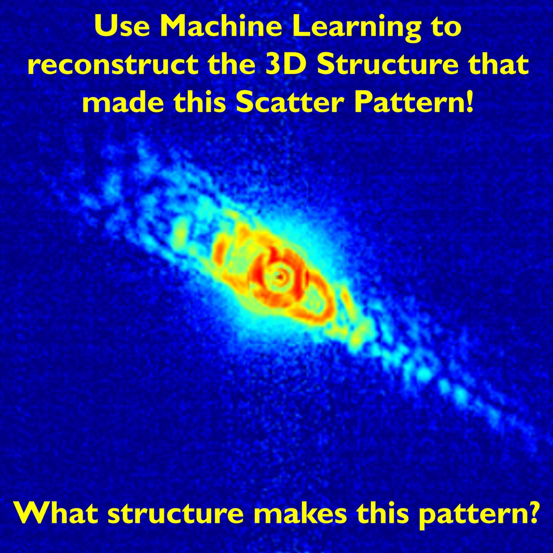
These new technologies only work as long as the underlying structures are near-perfectly made and the complexity and extremely small size of these components provide significant challenges in their characterization and imaging. Recently, a new imaging technique using extreme ultraviolet (EUV) light (light with a wavelength from ~10 - 120 nm) has emerged that has the potential to non-destructively image complex nanostructures in both space and composition. This technique, EUV lensless imaging, relies on the use of computer algorithms to process patterns of scattered EUV light from a structure or device, which are then used to reveal the final image of the object. This technique shows great promise for non-destructive imaging and characterization of nanostructures; however, we are only beginning to scratch the surface of its power for characterizing actual microelectronic device structures.
In this project, you will work closely with a diverse team of scientists and experts within imec’s advanced patterning department and materials characterization laboratory to help usher in a new era of EUV-based imaging of semiconductor materials. In your work, you will drive the development of machine-learning (ML) algorithms to enable and enhance lensless EUV imaging of technologically relevant semiconductor structures and devices. The algorithms you develop will push the boundaries of the state-of-the-art in EUV imaging, increasing resolution and enabling exotic paradigms such as buried-layer/depth-resolved imaging and chemical/elemental mapping. These algorithms will then be applied on real-world semiconductor structures to help enable a new paradigm in characterization and imaging that supports the development of evermore advanced devices.
Who You Are:
- Bachelor’s or Master’s degree in engineering, physics, mathematics, computer science, or a related field.
- Motivated, inquisitive student with a passion for learning new concepts and advancing current knowledge bases.
- Prior experience with optics, imaging processing and light propagation are considered strong advantages
- Familiarity with core machine learning architectures (e.g., PyTorch, Tensorflow, sci-kit-learn, etc.) is a strong plus
- Demonstrated programming experience is required (Python, MatLab, or equivalent language)
- Excellent written and oral communication in English
What We Provide:
- A diverse, dynamic working environment that employs international experts in nearly every discipline in semiconductors
- An extensive training network covering both technical and non-technical skillsets
- Participation in national/international conferences and workshops
- Fully funded scholarship (with benefits)
Type of work: 70% theory/simulation, 20% experiment, 10% literature
Interested?
Please supply an up-to-date CV as well as a motivational statement when submitting your application.
Required background: engineering, physics, math, com-science, optics, image processing & light propagation machine learning architectures (PyTorch, Tensorflow, sci-kit-learn,,..), programming experience is required (Python, MatLab,...), written & oral communication in English
Type of work: 70% theory/simulation, 20% experiment, 10% literature
Supervisor: Claudia Fleischmann
Co-supervisor: Janusz Bogdanowicz, John Petersen, Kevin Dorney
Daily advisor: Vitaly Krasnov, Bappaditya Dey
The reference code for this position is 2024-046. Mention this reference code on your application form.