CMOS: advanced and beyond
Discover why imec is the premier R&D center for advanced logic & memory devices.
Integrated photonics
Take a look at technologies for optical transceivers, sensors and more.
Health technologies
See how imec brings the power of chip technology to the world of healthcare.
Sensing and actuation
Explore imec’s CMOS- and photonics-based sensing and actuation systems.
Connectivity technology
Look into our reliable, high-performance, low-power network technologies.
More expertises
Discover all our expertises.
Research
Be the first to reap the benefits of imec’s research by joining one of our programs or starting an exclusive bilateral collaboration.
Development
Build on our expertise for the design, prototyping and low-volume manufacturing of your innovative nanotech components and products.
Venturing and startups
Kick-start your business. Launch or expand your tech company by drawing on the funds and knowhow of imec’s ecosystem of tailored venturing support.
Education and workforce development
Imec supports formal and on-the-job training for a range of careers in semiconductors.
Solutions
Use one of imec’s mature technologies for groundbreaking applications across a multitude of industries such as healthcare, agriculture and Industry 4.0.
Homo- and heterostructures with 2D single crystals by selective deposition for advanced logic applications
Leuven | More than two weeks ago
Gain a comprehensive understanding of chemical vapor deposition and utilize advanced industrial reactors to create heterostructures of 2D materials for future nano-electronic devices.
Novel two-dimensional (2D) materials, especially the semi-conducting transition metal dichalcogenides (TMDCs), offer advanced functionality in advanced and ultra-scaled integrated systems. In view of their compelling electronic, magnetic, and optical properties for a monolayer form, imec explores their integration for various applications and systems; in particular, for advanced CMOS technologies in a beyond-silicon roadmap.
The artificial fabrication of homo- and heterostructures, consisting of two or more 2D materials, provides an interesting pathway to preserve and tune the unique electrical properties for a given application. [1-4] However, the synthesis of 2D/3D homo- and heterostructures with industry compatible deposition techniques is still in the early stages.
The Goal
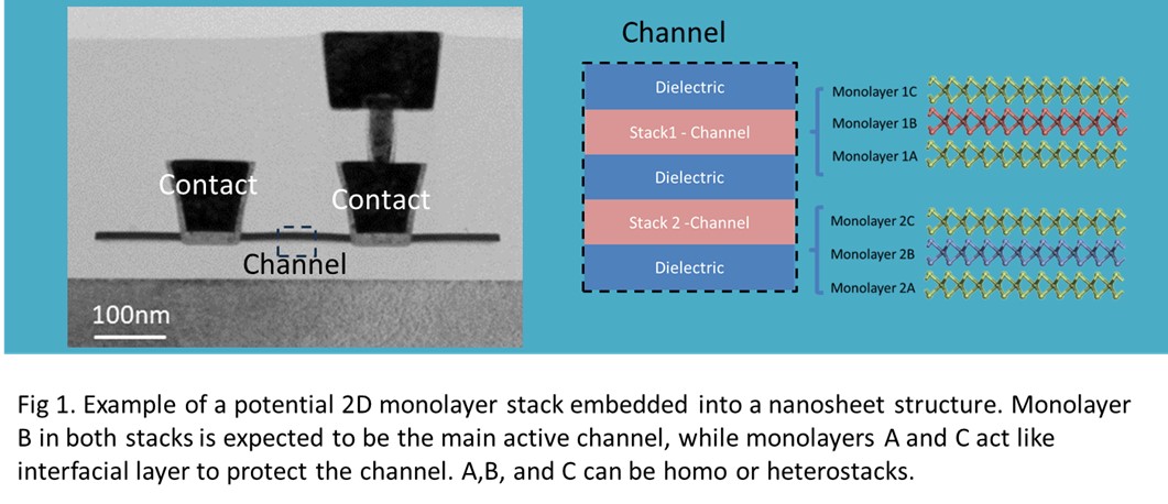
The main goal is to design novel deposition processes of homo- and heterostructures with monolayer thickness control that can be integrated into future sub-nanometer devices such as gate-all-around nanosheet field effect transistors (FETs) and atomically thin complementary FETs (CFETs). (Fig1.)
What you will do
In this PhD research project, you will explore the nucleation and growth behavior of TMDCs with monolayer thickness control by chemical vapor deposition (CVD) on other TMDCs and/or on amorphous dielectrics to create homo- and heterostructures with tunable and improved electrical performance.
During the PhD research, you are encouraged to:
- Develop fundamental understanding of TMDs growth mechanisms by combining experimental analysis via a complementary set of advanced characterization techniques with theoretical models.
- Design novel deposition concepts that ensure monolayer thickness control and enable stacking of 2D layers to form vertical heterostructures, based on the generated insight in the growth mechanisms.
- Critically review the existing literature in this novel research field and make analytical assessment of possible growth strategies.
This research will be conducted using imec's state-of-the-art 300mm clean room infrastructure. You will be a part of the 2D material growth team at imec, where you are supported by an international team of top researchers in different fields who will provide the necessary support to achieve your goals.
Your Training
In addition to the PhD track at the KU Leuven, you will:
- Learn how to operate 300mm industrial CVD reactors.
- Gain knowledge from different physical characterization techniques such as atomic force microscopy (AFM), X-ray photoelectron spectroscopy (XPS), Raman, photoluminescence (PL), Rutherford backscattering spectroscopy (RBS), transmission electron microscopy (TEM), scanning tunneling microscopy (STM), In-plane X-ray diffraction (In-plane XRD).
- Participate in preparing and aligning device fabrication flows for the electrical assessment of your samples together with device experts.
References
- Huang X, Liu C, Zeng S, et al. Ultrathin multibridge channel transistor enabled by van der Waals assembly. Adv Mater. 2021;33:2102201.
- Liu L, Liu C, Jiang L, et al. Ultrafast non-volatile flash memory based on van der Waals heterostructures. Nat Nanotechnol. 2021;16:874–881.
- H. Ago, S. Okada, Y. Miyata, K Matsuda, M. Koshino, K. Ueno, K. Nagashio. Science of 2.5 dimensional materials: paradigm shift of materials science toward future social innovation. Science and Technology of Advanced Materials, 2023, 23:1, 275-299.
- P. V. Pham, S. C. Bodepudi, K. Shehzad, Y. Liu, Y. Xu, B. Yu, X. Duan. Chem. Rev. 2022, 122, 6, 6514–6613.
Required background: Chemistry Science, Material Science, Physics Science, Electrical Engineering with emphasis on semiconductor technology, nanotechnology or related field.
Type of work: 5% literature, 5% theory, 90% experimental
Supervisor: Annelies Delabie
Co-supervisor: Pierre Morin
Daily advisor: Henry Medina Silva
The reference code for this position is 2024-017. Mention this reference code on your application form.