Reliability of high-voltage thin-film transistors for sensors and actuators
PhD - Leuven | More than two weeks ago
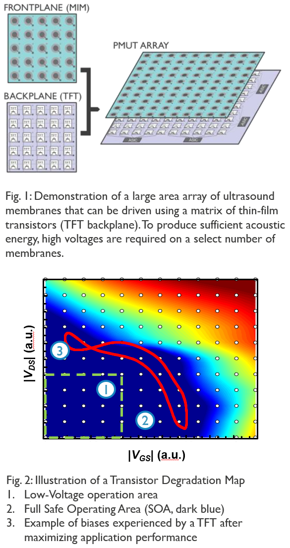
High-voltage low-temperature polysilicon (LTPS) thin-film transistors (TFT) are an excellent candidate for large-area high-voltage actuators and sensors: electrowetting-on-dielectric (EWOD) for lab-on-a-chip applications, medical and other ultrasound imaging and ranging, haptic feedback for health, robotics and automotive applications. Using this technology on thin and flexible substrates allows making artificial skins on autonomous machines and health patches on humans, which need to be flexible and curved to ensure natural movement and smooth operation.
Flexible TFTs operated at low voltages are already in production and are sufficiently reliable. However, many applications would greatly benefit from operating the TFTs at higher voltages. Unfortunately, the long-term reliability of the currently available TFTs under high-voltage stresses is still poorly understood. Furthermore, the impact of technological adaptations intended to improve the reliability under high-voltage stress should be carefully considered and balanced to avoid unnecessarily degrading device performance.
In general, TFT performance is hampered by charge carriers trapping in preexisting and newly generated defects. Especially the latter mechanism is reported to be significant in TFTs and has been suggested to be caused by hydrogen release and diffusion within the device. The student will employ electrical characterization techniques and physics-based modeling to describe the kinetics (i.e., the time dependence) of all aging degradation mechanisms and their dependences on device biases, bias frequency, temperature and mechanical strain. These degradation models should allow the student to define a Safe Operating Area (SOA) of the TFTs and compact models for further electrical circuit simulations.
Furthermore, this PhD project also offers the possibility to apply this understanding within the frame of joint project with an industrial partner. On one hand, proposed optimizations of technological parameters (e.g. layer thicknesses, …) can be implemented by the fab partner(s) allowing direct experimental verification and deeper understanding of the fundamental degradation mechanisms. On the other hand, the HV-TFT devices can be implemented within the intended circuit building blocks; their reliability can be monitored during a realistic workload scenario in our internal characterization labs. Throughout the project, the student will have access to design, simulate and layout tools using the in-house PDK.
Selected references:
https://doi.org/10.1002/sdtp.16764
https://ieeexplore.ieee.org/stamp/stamp.jsp?arnumber=4016327
https://doi.org/10.1002/jsid.873
https://ieeexplore.ieee.org/stamp/stamp.jsp?arnumber=4734622
https://ieeexplore.ieee.org/stamp/stamp.jsp?tp=&arnumber=8353540

Required background: Semiconductor Device and Modelling and circuit understanding
Type of work: 50% device simulation, 30% device characterization and 20% circuit simulation and measurement
Supervisor: Jan Genoe
Daily advisor: Ben Kaczer, Florian De Roose
The reference code for this position is 2025-178. Mention this reference code on your application form.
