In-situ study of wet-chemical etching of HAR nanostructures
PhD - Leuven | More than two weeks ago
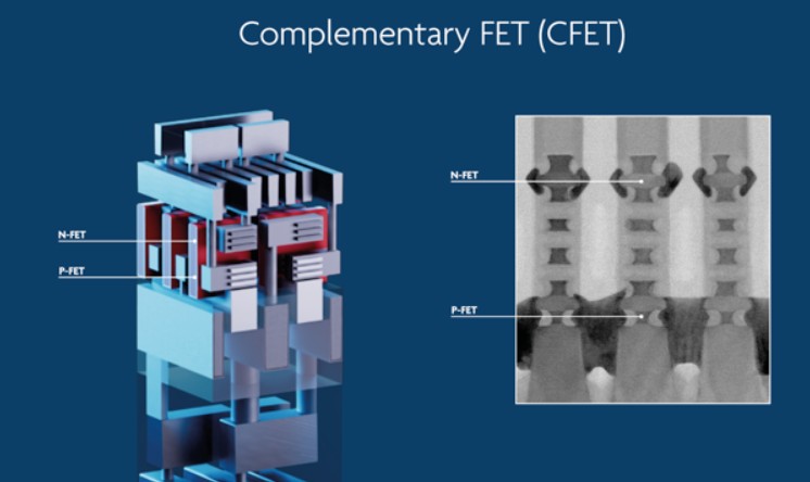
As CMOS scaling approaches its physical limits, complementary FET (CFET) with vertically stacked devices has emerged as a promising candidate to reduce footprint and enhance performance for advanced technology nodes. However, the CFET architecture substantially increases process complexity, requiring precise patterning of high aspect ratio (HAR) structures with multiple materials in the stacks. There remains a significant gap when it comes to understanding the intrinsic material properties and etching behavior, particularly on HAR structures. Understanding wetting and wet-chemical etching mechanisms on HAR nanostructures enables precise process control that is essential for device performance, reliability, and scalability.
Extensive work has been done over the past decades in characterizing the etching of blanket non-patterned thin films. However, the direct transfer of such knowledge to ‘real’ substrates patterned with HAR structures introduces additional complexities, such as surface roughness, plasma-induced damage and the presence of multiple materials, which often lead to unexpected observations that are not well understood at a fundamental level.
In earlier work, we applied advanced metrologies to probe in-situ nanoscale physicochemical interactions across various applications, including nanoscale wetting phenomena1–3, capillary-induced self-assembly of nanostructures4, and the mechanisms of nanoscale silicon etching5. Building on these insights, this project will further investigate how different structural geometries, pattern densities, surface chemistries and wet solutions influence wet chemical etching processes. The PhD project is structured into two phases. The first phase aims to experimentally characterize the material and surface differences, establishing correlations with etch rates in both blanket and patterned materials. In the second phase, an in-situ study will be conducted using a flow cell integrated into the ATR-FTIR system to characterize the dynamic changes in surface chemistries and the solution near the surface.
The successful candidate should have a solid background in (physical) chemistry, physics or material science, with strong problem-solving skills and good writing and oral communication skills.
Contact: XiuMei Xu (xiumei@imec.be), Harold Philipsen (Harold.Philipsen@imec.be)
1. Xu, X. et al. Capturing wetting states in nanopatterned silicon. ACS Nano 8, 885–893 (2014).
2. Vrancken, N. et al. Superhydrophobic Breakdown of Nanostructured Surfaces Characterized in Situ Using ATR-FTIR. Langmuir 33, 3601–3609 (2017).
3. Vrancken, N. et al. In-situ ATR-FTIR for dynamic analysis of superhydrophobic breakdown on nanostructured silicon surfaces. Sci. Rep. 8, (2018).
4. Vrancken, N. et al. Nanoscale Elastocapillary Effect Induced by Thin-Liquid-Film Instability. J. Phys. Chem. Lett. 11, 2751–2758 (2020).
5. Aabdin, Z. et al. Transient Clustering of Reaction Intermediates During Wet Etching of Silicon Nanostructures. Nano Lett. 17, 2953–2958 (2017).
Required background: chemistry, physics, material science, engineering
Type of work: 50% experiments, 40 % analysis and modeling, 10% literature
Supervisor: Stefan De Gendt
Co-supervisor: XiuMei Xu
Daily advisor: XiuMei Xu, Harold Philipsen
The reference code for this position is 2026-119. Mention this reference code on your application form.