[NanoIC topic] Understanding the Hidden Chemistry of Vapor-Phase Reactions to Enhance Photoresist Materials for EUV Lithography
PhD - Leuven | More than two weeks ago
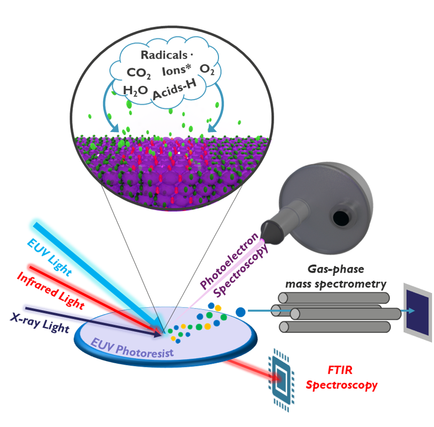
Extreme ultraviolet (EUV) lithography is a cornerstone technology that enables the production of the most advanced nano-electronic devices that power our society and daily lives. Central to the power of EUV lithography is the imaging material, the photoresist, that transforms a nanoscale optical image into a chemical image that serves as the “blueprint” for advanced transistor structures. From a materials perspective, improving this lithographic “blueprint” is typically achieved via material optimization of the photoresist itself, via direct chemical or process modification. However, recent studies have indicated that a largely unexplored realm of photoresist chemistry, specifically, the interaction of photoresists with vapor-phase chemistries can substantially alter photoresist performance [1-3], potentially providing an untapped avenue for improving photoresist performance. These vapor-phase chemistries occur at critical steps in the EUV lithographic process, such as environmentally-mediated chemical reactions during processing steps [2-3] or enhancing lithographic material performance with vapor or plasma-etching [4-5].
While promising, the chemical and physical mechanisms that underly vapor-phase enablement of photoresists are largely unknown, thus preventing mechanism-informed optimization of EUV lithography performance. Addressing this knowledge gap demands a coordinated, fundamentally-focused approach that bridges the domains of optical/EUV lithography, chemical spectroscopy, and vapor-material interface reactions to elucidate the complex mechanisms at play.
The objective of this PhD research is to experimentally characterize and uncover the chemical and physical mechanisms that underly the reactions of vapor-phase components (molecules, ions, etc.) with EUV photoresist materials and identify pathways that enhance (or hinder) their performance. In this interdisciplinary project, you will work at the interface between light-matter interactions, material design, and interface-mediated chemical reactions to uncover the hidden chemistry of vapor-phase reactions that influence photoresist performance. This ambitious project will be supported by imec’s advanced LAB and FAB infrastructure comprised of chemical characterization techniques and spectroscopies, lithography exposure and processing tools, and associated metrologies. This infrastructure is augmented by several unique toolsets, such as the imec AttoLab (for EUV spectroscopy using high-harmonic EUV sources) and an EUV exposure system with in-situ FTIR and mass spectrometry capabilities for studying photoresist chemistry in a controlled vapor environment (the imec BEFORCE tool). You will also work closely with experts in EUV lithography, EUV materials, vapor/plasma chemistry, and chemical modelling to provide a wholistic understanding of this uncharted realm of EUV photoresist chemistry.
As a PhD candidate within imec's Ångström Patterning Department, you will,
- Perform EUV lithography exposures using FAB and LAB equipment and develop informed process flows to test hypotheses involving photochemical and vapor-phase mechanisms of EUV patterning materials.
- Conduct a comprehensive FAB- and LAB-based characterization of photoresist materials at all steps in the lithographic process chain (pre/post exposure and pre/post development).
- Develop a strong technical skillset for diverse characterization techniques (e.g., FTIR, AFM, XPS, mass spectrometry, etc.).
- Correlate chemical and mechanistic observations with patterning performance.
- Critically analyze spectroscopic and imaging data with respect to material and process variation.
- Presenting your findings at conferences, internal meetings, and gaining exposure to key players in the global semiconductor community.
- Assist in teaching labs sessions and/or monitoring examinations of relevant courses at the bachelor’s and master’s level at KU Leuven (<5% of total time).
- Material processing to broaden your technical skillsets.
What We Offer
We offer you the opportunity to join one of the world’s premier research centers in nanotechnology at its headquarters in Leuven, Belgium. With your talent, passion and expertise, you’ll become part of a team that makes the impossible possible. Together, we shape the technology that will determine the society of tomorrow.
We are aware that your valuable contribution makes imec a top player in its field. Your energy and commitment are therefore appreciated by facilitating your further career development:
- Imec values a cooperative spirit. What does it mean for you? You can easily collaborate across teams and fields with our 6000+ colleagues. Thus, directly learn from the many leading experts in nanotechnology, metrology, system architecture, etc. and accelerate your research.
- Extensive support infrastructure (automated measurement department, leading edge metrology department, public funding department, etc.) that will allow you to concentrate on your research.
- Imec is the crossroad where all semiconductor players meet to tackle fundamental research questions and technology bottlenecks. This allows you to build a unique network within academia and industry that you will be able to leverage for any future career.
- Belgium and imec value family and support young researchers extensively (childcare for the youngest, flexible working hours understanding that family affairs are of high importance).
- Through imec.academy, 'our corporate university', we actively invest in your development to further your technical and personal growth.
- We are proud of our open, multicultural, and informal working environment with ample possibilities to take initiative and show responsibility. We commit to supporting and guiding you in this process, not only with words but also with tangible actions.
Who You Are
- You have (or will soon obtain) a Master’s degree in chemistry, physics, material science, nanoscience, or chemical engineering. A focus on (EUV) lithography and chemical spectroscopies of thin films is a plus.
- Prior research in spectroscopy, chemical analysis, materials science, and/or (EUV) lithography is highly desired.
- Proficiency in scientific programming (Python, Matlab, C, etc.).
- Excellent lab skills with attention to detail and safety protocols.
- Strong problem-solving skills, with a knack for innovative thinking.
- Proficient in data analysis and interpretation.
- Ability to work both independently and collaboratively in a team-oriented setting.
- You are creative, result-driven, and can meet deadlines with quality output.
- You are a clear and effective communicator. Strong language skills in English are required for imec’s diverse working environment.
References for Further Reading
[1] Nye, R. A., Van Dongen, K., De Simone, D., Oka, H., Parsons, G. N., Delabie, A. “Enhancing Performance and Function of Polymethacrylate Extreme Ultraviolet Resists Using Area-Selective Deposition”, Chem. Mater. 35 (5), 2016-2026 (2023).
https://doi.org/10.1021/acs.chemmater.2c03404
[2] Castellanos, et al. “EUV Metal Oxide Resists: Impact of the Environment Composition on CD during Post-Exposure Delay”, Proc. SPIE 12957, 1295707 (2024).
https://doi.org/10.1117/12.3010921
[3] Dorney, K. M., et al. “Fundamental Understanding of Exposure and Process Chemistry for Enhanced Lithography and Stability of Metal Oxide Resists”, Proc. SPIE 13428, 134281C (2025). https://doi.org/10.1117/12.3051260
[4] Kenane, et al. “Dry Deposition and Dry Development of Metal Oxide Based Photoresist”. J. Photopolym. Sci. Technol.37 (3), 257-262 (2024).
https://doi.org/10.2494/photopolymer.37.257
[5] Seok, J.-H., Kim, J., Ji, H., Lee, J., Yoon, K., Mo Sung, M., Ahn, J. “A Dry Development Process for Vertically Tailored Hybrid Multilayer EUV Photoresist: Chemical Vapor Development (CVD)” Proc. SPIE 13215, 1321502 (2024). https://doi.org/10.1117/12.3034596
Required background: chemistry, physics, material science, nanoscience, or related
Type of work: 80% Experimental, 10% simulation, 10% literature
Supervisor: Annelies Delabie
Co-supervisor: Danilo De Simone
Daily advisor: Kevin Dorney
The reference code for this position is 2026-191. Mention this reference code on your application form.