From television screens to smartphones, automotive lighting and wearables, OLEDs are turning up in an increasing number of applications. OLED displays can be made thin and flexible, they show excellent optical performance and can be scaled up for large sizes. But will they also favor the evolution towards ever higher display resolution, and as such realize new types of applications such as virtual or augmented reality devices? Pawel Malinowski and TungHuei Ke, senior researchers at imec, explain how imec and Holst Centre address these new needs. They identify photolithography as a key enabling technology for making the next-generation high-resolution (AM)OLED displays.
OLED technology gaining share in the display market
For more than half a century, cathode ray tubes have been the most popular display technology used in televisions and computers, until being displaced by plasma and liquid crystal device (LCD) technologies. These technologies were at the origin of the flat panel display, which now is not only commonplace in the home and office, but also in automotive, mobile and multimedia devices. Since 2010, the plasma display market has lost ground, in favor of a new competitor for LCD technology: OLED technology. Pawel Malinowski: “This newcomer has already gained significant market share in the display market (9.3% in 2015) and its share is continuously increasing. OLED displays are now mass produced for mobile phones, tablets, TVs and wearables. IDTechEx forecasts the market for all types of OLED displays to reach nearly 16 billion dollar in 2016 and to grow to 57 billion dollar in 2026.”
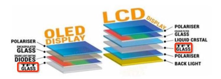
TungHuei Ke: “OLEDs and LCDs are based on different technologies. An OLED is a multilayer device where functional multilayer organic semiconductors are sandwiched between the electrodes. The electrons and holes can be injected under voltage bias and recombine to generate excitons in the emission layer. Photons can be generated via the energy relaxation of the excited emission molecules. The emission color can be fine-tuned by choosing the emission molecule and device structure. This leads to a wider color space and more accurate color point compared to LCDs. Unlike LCD, which uses liquid crystal material as a switch to control the light emission intensity, OLED is a self-emitting device. This results in important advantages such as very fast response time, high refresh rate, infinite contrast ratio (true black) and simpler panel structure compared to LCD technology. The OLED is a current-driven device. In an active matrix OLED display, the individual subpixels can be driven independently by the corresponding pixel driving engine. Due to the simpler panel structure of OLED display, the OLED panel can also be made very thin, making it more suitable for flexible, rollable or even stretchable displays. Because of the superior mechanical properties of the flexible OLED displays, it can be applied to different wearable electronics with various form factor. More and more companies in the display industry decided to go for mass production of OLEDs, targeting 2018 for the next-generation portable electronic devices.”

Device structure comparison between OLED and LCD (source: https://www.linkedin.com/pulse/20140814014849-147801316-what-s-the-difference-of-ips-oled-ltps)

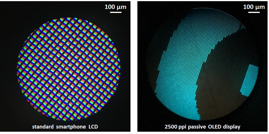
User experience of an LCD vs. OLED display. The picture shows microscopy images of an LCD display and of imec’s mono-color 2500ppi passive OLED display. On the OLED display, significantly more pixels can be packed in the same area.
Towards 8K resolution displays
The display industry is one of the most innovative. Novel products with new form factors and use cases are rapidly being introduced, especially in AMOLED displays. One example is near-eye display devices, including virtual reality and augmented reality devices. Pawel Malinowski: “At the same time, the race for higher resolutions does not seem to slow down. Today’s products require OLED displays of high pixel density, i.e. around 200 pixels per inch (ppi) for 4K (3840x2160 pixels) television, and 500ppi for full high-definition (1920x1080 pixels) mobile devices. Display makers propose to further increase the display resolution towards 8K (7680x4320 pixels). Studies have pointed out that this would facilitate depth sensation, and as such create the perception of a 3D scene in a flat TV panel. Depending on the display type, 8K resolution translates into different pixel pitch requirements. For example, for a 5.5 inch smartphone display, this translates into a pixel pitch below 20 micrometer. For a micro-display, (0.5 inch), a pixel pitch as small as 2 micrometer would be required.”
Pixel pitch requirements at 8K resolution for different display types (television, tablet, smartphone and micro-display/head-mounted display).
Photolithography, a key technology
One of the major challenges in producing high-resolution OLED displays is the patterning of very small OLED pixels. Current methods for patterning organic semiconductors include shadow masking and inkjet printing. Even though these methods are very efficient for small displays with low resolution (below 500 ppi), they are not suitable for high-resolution patterning on large-size substrates. In the shadow masking approach, for example, a thin sheet (mask) of metal with holes in it is placed over the substrate. The organic molecules travel through the holes before ending up on the substrate. Pawel Malinowski: “This method is capable of offering pixel pitch in the range of 20 micrometer. Still, the display size and production yield pose practical challenges due to mask bending and cleaning procedures. Also, using masks results in a cross-fading area about 15 to 20 micrometer between RGB stacks. This means that at higher resolutions, the aperture area – or the area that actually emits light – suffers dramatically.”
Display manufacturers are therefore eagerly looking for a technique that enables submicron patterning of RGB OLEDs on small and large-size substrates, in a cost-effective way. And this is where photolithography enters the scene. This CMOS-like fabrication route allows practically unlimited substrate size and resolution. Moreover, the necessary equipment is already in use, and that on an industrial scale. TungHuei Ke: “Applying this patterning technique on organic materials is however not straightforward. The standard chemicals (photoresists, developers, strippers) used to pattern silicon dissolve or contaminate the fragile organic semiconductor material. Conventional OLED devices also degrade largely under standard process conditions in photolithography such as ambient air and UV light exposure. Alternative resist materials in certain process conditions have been proposed, such as frozen CO2 or fluorinated resists. But these materials present challenges in terms of waste treatment, tool compatibility and up-scalability for production.”
i-line photoresists – an imec and Fujifilm approach
Imec and Fujifilm have been working on non-fluorinated, chemically amplified photoresist systems compatible with i-line photolithography (i.e., using 365nm UV light for exposure). In 2013, they demonstrated for the first time the feasibility of this technology. Since then, the team reached several state-of-the-art milestones showing that the method is capable of high-resolution patterning on large substrates. Pawel Malinowski: “In 2014, we showed double-color OLED arrays patterned with 200 micrometer sub-pixel pitch. In 2015, we successfully demonstrated RGB OLED arrays with 20 micrometer sub-pixel pitch and 640ppi resolution. And recently, we used the technique to produce double-color OLED arrays with 10 micrometer sub-pixel pitch and 1250ppi resolution. With this unique, cost-effective and disruptive approach, we address not only the OLED chemical compatibility but also fab compatibility and up-scalability.” Indeed, there is no need for additional capital investment since existing i-line exposure systems can be used for the new technology.
A 1250ppi multi-color OLED display
To verify patterning, Fujifilm and imec used test structures fabricated in a common-contact configuration. In such a simple structure, the anode (ITO) and cathode (Ag) are shared by all pixels in an array. Processing of the test structures is done on 3x3cm2 glass substrates with pre-patterned bottom contact lines. For each OLED color, a small-molecule multilayer stack containing various organic semiconductor is thermally evaporated on top of a SiN edge-cover layer (ECL), a layer that is provided over the step and edge areas. Patterning is achieved with photolithography of each color on top of the SiN ECL. After exposing the i-line photoresist through the photomask, the uncovered OLED stack is removed using reactive ion etching.
Schematic cross section of an RGB OLED array test structure.
TungHuei Ke: “In this way, we are able to achieve a high aperture ratio of 85% in a 20 micrometer pitch array, which corresponds to 640ppi resolution. For comparison, the aperture ratio of the commercialized 500ppi OLED display is around 18%. Achieving such a high effective emission area is one of the strengths of this photolithography technique. This is a crucial requirement for near-eye display applications in the field of virtual/augmented reality. The smaller portion of black area (smaller inter-pixel spacing) would increase the image quality significantly for better immersive experience. Furthermore, a higher aperture ratio of the emissive pixel leads to lower current density for the same brightness level. This could greatly increase the OLED operational lifetime. We also checked for any degradation effects. Patterning of fragile OLED stacks is known to degrade for example the photo-electric conversion. After optimizing photoresist, process conditions and OLED device structures, opto-electrical characterization of single-color devices indicates little influence of the patterning.” Pawel Malinowski: “In our latest achievement, we fabricated 1900x600 sub-pixel passive displays with patterned side-by-side arrays of red and blue stacks. For both colors, we observed uniform emission.
In this configuration, an array pixel consists of 4 sub-pixels (two red, two blue), and the full-color pitch of 20 micrometer (or sub-pixel pitch of 10 micrometer) amounts to 1250ppi. Together with Fujifilm, we are currently working on three-color OLED arrays with 10 micrometer sub-pixel pitch.”
Demonstration of imec and Fujifilm’s high-resolution OLED displays. (Left) passive display with one OLED color and a resolution of 2500ppi; (center) passive display with two OLED colors and a resolution of 1250ppi; (right) microscope image of a detail of the two-color array showing electroluminescence of 10 micrometer pitch OLED pixels.

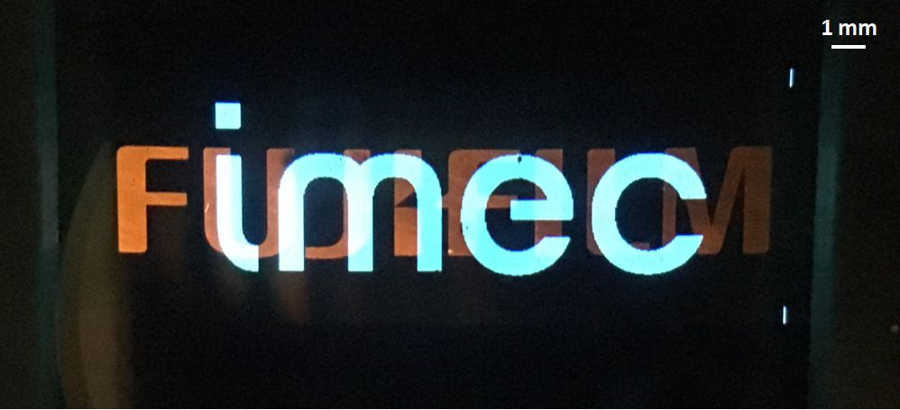
Detailed image of the passive display with orange/blue OLED colors and 1250ppi resolution.
The path towards next-generation displays
As these results clearly show, photolithography provides a cost-effective, disruptive fabrication process for RGB OLEDs. With a resolution as high as 1250ppi and a sub-pixel pitch of 10 micrometer, the patterning of multi-color OLED arrays for above-4K smartphone displays becomes feasible. But there are other issues that need to be solved for these displays to enter the market. For example, the common-contact configuration used in RGB test structures is not ideal for multi-color arrays. Pawel Malinowski: “In reality, the turn-on voltage of different OLED emission layers varies. Therefore, in a next step, this process will be integrated on top of a thin-film transistor (TFT) backplane, where each color will be driven separately. And there is degradation in lifetime, currently one of the most important concerns in novel manufacturing techniques. This requires a more extensive study of the degradation phenomena of the new patterning process.”
All these new needs are addressed in imec and Holst Centre’s flexible display program. This program started four years ago and works towards a cost-effective production of the next-generation flexible AMOLED displays. The team looks into foil handling solutions, into TFT back-plane processing and into the processing of thin barriers needed for protecting the OLEDs. They research a number of key technologies that will reduce power consumption, extend lifetimes, cut manufacturing costs and further increase the performance of these soon-to-be ubiquitous displays.
Published on:
28 December 2016


