The near-term logic technology roadmap: three generations of GAA nanosheet technology
Leading foundries and IDMs are advancing toward mass production of the 2nm (or equivalent) technology node, in which gate-all-around (GAA) nanosheet transistors play a central role. The GAA nanosheet device architecture has been introduced as a successor to FinFET technology to allow further downsizing of SRAM and logic standard cells.
The main feature of the GAA nanosheet device is the vertical stacking of two or more nanosheet-shaped conduction channels, with one stack for p and one stack for n devices contained in a logic standard cell. This configuration allows designers to shrink logic standard cell height further, which is defined as the number of metal lines (or tracks) per cell times the metal pitch. Designers can also choose to make the channels wider, trading cell height for larger drive current. In addition to area scaling, GAA nanosheet transistors offer another advantage over FinFETs: the gate surrounds the conduction channels on all sides, improving gate control over the channel, even for short channel lengths [1].
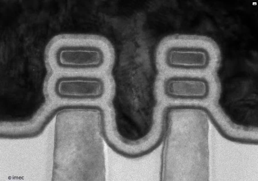
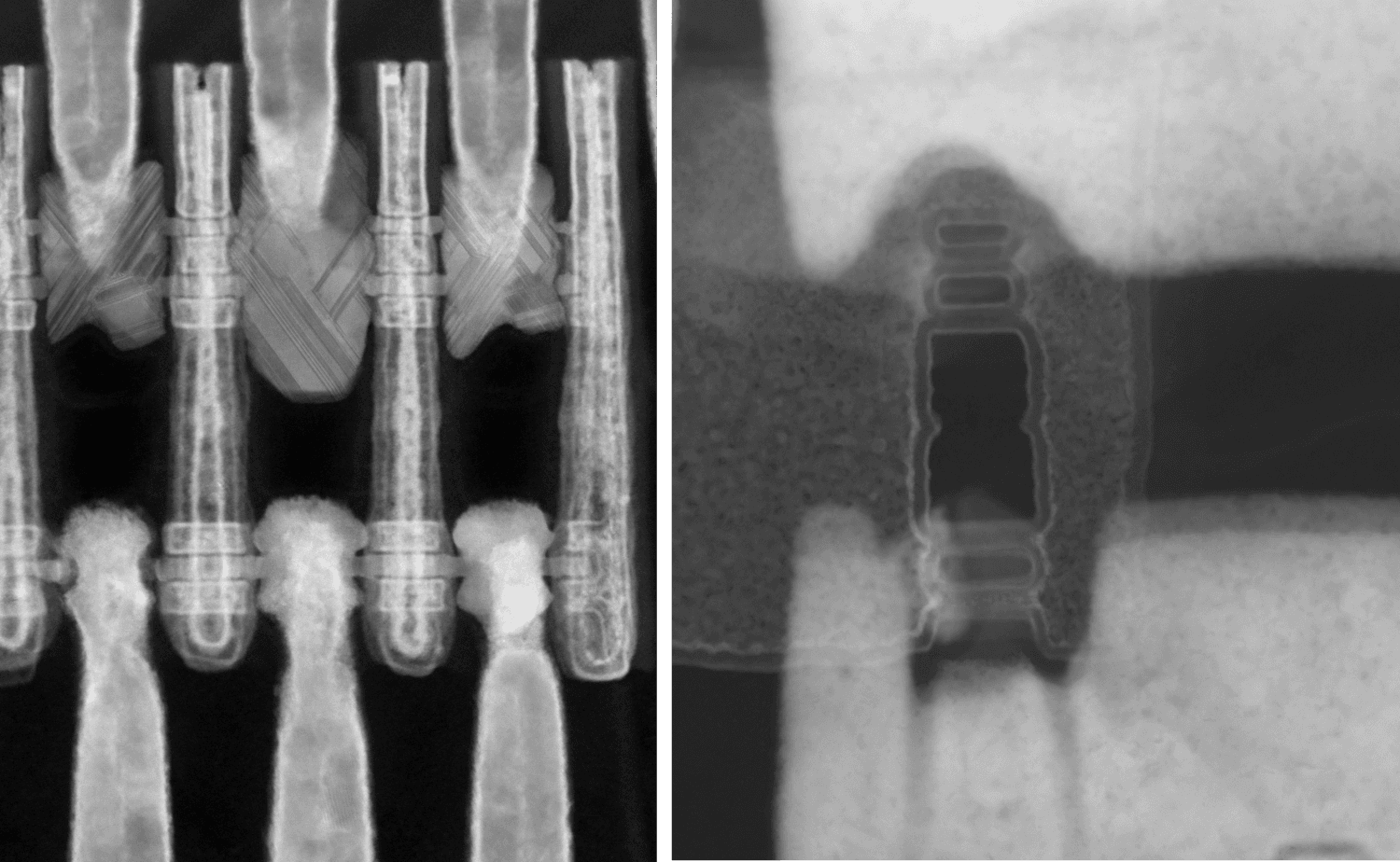
Figure 1 – TEM image of GAA nanosheet devices.
Do you want regular updates on imec’s semiconductor research?
GAA nanosheet technology is expected to last for at least three technology generations before chip makers transition to the complementary FET (or CFET) technology.
Because of its nMOS-pMOS vertically stacked structure, the integration complexity of the CFET is significantly higher than that of regular nanosheet devices. This makes CFET mass production feasible only from the A7 node onwards, according to imec’s roadmap. This means the GAA nanosheet era must be stretched to at least the A10 technology node, where cell heights are expected to be as small as 90nm. Shrinking GAA nanosheet-based standard cells without compromising performance is, however, challenging.
This is where the forksheet device architecture may bring relief, a non-disruptive technology with larger scaling potential than regular GAA nanosheet technology.
The forksheet: scaling booster to extend the GAA nanosheet ‘family’ to A10
In 2017, imec introduced the forksheet device architecture, first as a scaling booster for SRAM cells [2], and later as a logic standard cell scaling enabler [3]. Distinctive of its first implementation is a dielectric wall that is put in between nMOS and pMOS devices before gate patterning. As this wall is placed in the middle of a logic standard cell, the architecture is referred to as the ‘inner wall’ forksheet. The wall physically isolates the p-gate trench from the n-gate trench, allowing a much tighter n-to-p spacing than possible with either FinFET or nanosheet devices. This allows further cell area scaling (up to 90nm cell height) while still offering a performance gain. In this ‘inner wall’ configuration, the sheets are controlled by a tri-gate forked structure, to which the device owes its name.

Figure 2 – TEM image of inner wall forksheet devices.
At VLSI 2021, imec demonstrated the manufacturability of the 300mm inner wall forksheet process flow [4]. Electrical characterization of the fully functional device confirmed that the forksheet is the most promising device architecture to extend the logic and SRAM nanosheet scaling roadmaps into the A10 node. Since the integration flow reuses much of the nanosheet production steps, the technology evolution from nanosheet to forksheet can be regarded as non-disruptive.
Manufacturability of the ‘inner wall’ forksheet is being challenged
Despite successful hardware demonstrations, a few concerns about manufacturability remained, making imec rethink and improve its initial forksheet device architecture. The main challenge relates to the manufacturability of the inner wall itself. To achieve 90nm logic standard cell height, the dielectric wall needs to be extremely thin, in the 8-10nm range. But, being fabricated early in the device process flow, the wall is exposed to all subsequent front-end-of-line (FEOL) etching steps that may further thin the wall, putting considerable demands on the choice of the material from which the wall is made. Also, to enable process steps specific to either n or p (such as p/n source/drain epi), a dedicated mask must precisely land on the thin dielectric wall, challenging p/n mask alignment.
In addition, 90% of the devices in real-life implementations have a common gate for the n and p channels. In standard cells with inner wall forksheet devices, the dielectric wall obstructs such a p-n connected gate. This is, unless the gate is made higher to cross the wall, which in turn increases parasitic capacity.
Finally, chip makers are concerned about the tri-gate architecture, where the gate only surrounds the channels on three sides. Compared to GAA structures, the gate risks losing control over the channel, especially at short channel lengths.
The ‘outer wall’ forksheet: a dielectric wall at the cell boundary
At the 2025 Symposium on VLSI Technology and Circuits (VLSI 2025), imec researchers presented a novel forksheet device architecture, which they named the ‘outer wall’ forksheet [5]. They have shown through TCAD simulations how this outer wall forksheet improves on its previous design by providing reduced process complexity and superior performance while preserving area scalability.
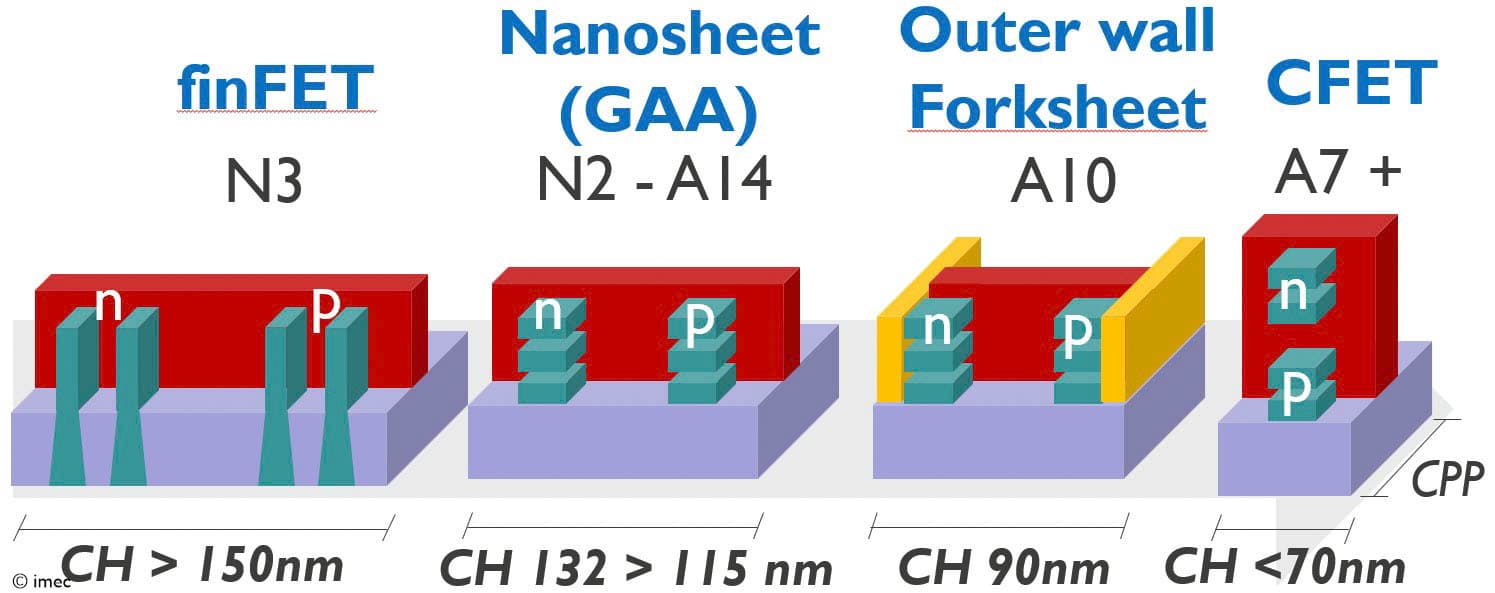
Figure 3 – Imec’s logic technology roadmap, showing the extension of the nanosheet era from 2nm to A10 node with the outer wall forksheet, before transitioning to CFET for A7 and beyond (as presented at VLSI 2025).
The outer wall forksheet places the dielectric wall at the standard cell boundary, turning it into a p-p or n-n wall. This allows each wall to be shared with its neighboring standard cell and to be made thicker (to around 15nm) without compromising the 90nm cell height.
Another distinctive feature is the wall-last integration approach. The overall process flow starts with forming a wide Si/SiGe stack – a step that recurs in any GAA technology. The Si layers of this stack will form the nanosheet-shaped conduction channels, after SiGe has been etched away during the nanosheet channel release step. The dielectric wall will eventually divide this stack into two, with two FETs of similar polarity ending up at opposite sides of the wall. The wall itself is processed near the end of the integration flow, i.e., after nanosheet channel release, source/drain etch back, and source/drain epi growth. A replacement-metal-gate (RMG) step completes the integration flow.
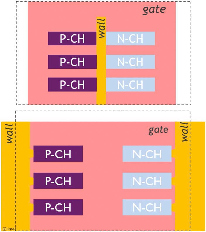
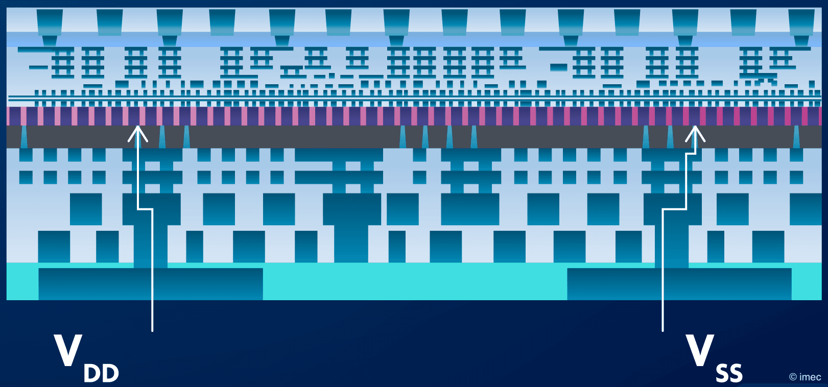
Figure 4 – Schematic representation of (top) inner wall and (bottom) outer wall forksheet architectures (as presented at VLSI 2025).
5 key improvements of the outer wall forksheet over inner wall designs
Inner and outer wall forksheets have two advantages in common over GAA nanosheet devices. In terms of area scaling, they are both capable of achieving 90nm logic standard cell height at the A10 node, which compares favorably with the 115nm cell height in A14 nanosheet technology. A second common advantage is a reduced parasitic capacitance: the two FETs on opposite sides of the wall (either n and p in case of the inner wall, or n and n/or p and p in case of the outer wall) can be put much closer together than in a scaled nanosheet-based cell without causing a capacitance problem.
In addition, the outer wall forksheet promises to outperform the inner wall design in five key aspects.
First, the dielectric wall is spared several aggressive FEOL steps because of the wall-last integration approach. Therefore, it can be made from mainstream silicon dioxide. During the wall-last process step, the wall is formed by trench formation in the wide Si/SiGe stack and SiO2 dielectric fill.
Second, since the wall is placed at the cell boundary, its width can be relaxed to about 15nm, leading to process simplification.
Third, the gates of the n and p devices within one standard cell can now be easily connected without having to cross the dielectric wall.
Fourth, the outer wall forksheet is expected to offer superior gate control over an inner wall device, linked to the ability to form a Ω-gate instead of a tri-gate forked structure. The wider dielectric wall makes it possible to do a few-nm etch-back of the wall during the final RMG step. This allows the gate to partially wrap around the fourth edge of the channel, resulting in a W-shaped gate with increased control over the channel. From TCAD simulations, imec researchers found that etching away 5nm of the dielectric wall was most optimal, boosting the drive current by ~25%.

Figure 5 – The effect of wall etch-back on gate formation: from tri-gate to Ω-gate, and to GAA (as presented at VLSI 2025).
The fifth aspect is linked to the potential of the forksheet integration flow to provide full channel strain, an additional performance booster benefiting drive current. In general, full channel strain can be obtained by implementing source/drain stressors. This method has proven very effective in (p-type) FinFETs but challenging to obtain in GAA nanosheet and inner wall forksheet device architectures. Conceptually, the idea is to incorporate Ge atoms into the source/drain region. Being larger than the Si atoms, they induce a compressive strain into the Si channel, boosting the mobility of the charge carriers.
The reason why fully effective source/drain stressors can be achieved in outer wall forksheet devices is because of the wall-last approach. Before the wall is made, a hard mask continues to cover the middle part of the wide Si/SiGe stack, the part that later serves to form the wall (Figure 6). The ‘Si spine’ underneath this hard mask can now serve as a seed crystal during the source/drain epi growth, acting as a Si ‘template’ that continues from one gate’s channel to the next. This is similar to the Si subfin in FinFET technology: imagine turning the source/drain epi module 90° (Figure 7). Without such a Si crystal template, vertical defects would form at the source/drain epi interfaces, which would lift the compressive strain formed within the Si channels.
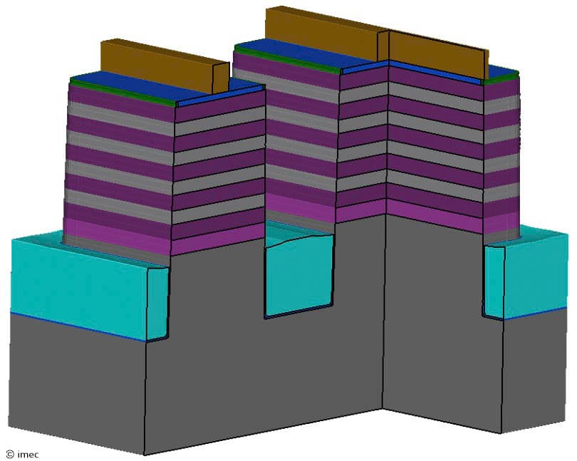
Figure 6 – At the start of the outer wall forksheet process flow, a ‘pre-wall’ hard mask (brown) is deposited on top of the wide Si (gray)/SiGe (purple) layer stack. This way, a Si ‘seed crystal’ underneath the hard mask supports source/drain epi growth (as presented at VLSI 2025).
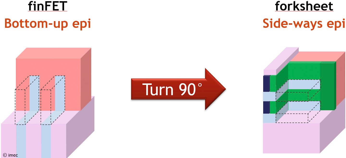
Figure 7 – The Si spine in the outer wall forksheet (right) provides a continuous Si crystal template from one gate’s channel to the next. This is conceptually similar to the Si subfin in FinFET technology (left) (as presented at VLSI 2025).
Outer wall forksheet in SRAM and ring oscillator designs: a PPA benchmark
Finally, imec conducted a benchmark study to quantify the power-performance-area (PPA) benefits of the outer wall forksheet.
The area benefit over nanosheet architectures becomes apparent when comparing the areas of the A10 outer wall forksheet and the A14 nanosheet-based SRAM bit cells. Layouts reveal a 22 percent area reduction for outer wall forksheet-based SRAM cells, arising from the p-p and n-n spacing reduction that comes on top of a scaled gate pitch.
Another key metric for performance evaluation is the simulated frequency of a ring oscillator, expressed as the ratio of the effective drive current and the effective capacitance (Ieff/Ceff). Simulations show that for the A10 node, an outer wall forksheet is needed to remain on par with the frequency metrics of the previous A14 and 2nm nodes, provided that full channel stress can be enabled in all these device structures. Implementing full channel stress in nanosheet (2nm and A14) and inner wall forksheet devices has proven challenging, its absence leading to an estimated 33 percent loss of drive current. The ability to implement effective source/drain stressors in outer wall forksheet devices is, therefore, expected to yield a further performance advantage in ring oscillator designs.
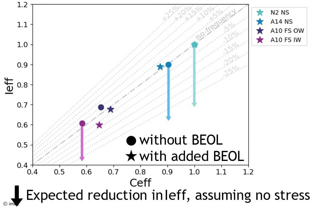
Figure 8 – Ring oscillator simulation results (with and without back-end-of-line (BEOL) load) (as presented at VLSI 2025).
Outlook and conclusion
The forksheet device architecture was introduced by imec to extend the nanosheet-based logic technology roadmap into the A10 technology node, in anticipation of CFET being ready for mass production. Manufacturability issues caused imec to abandon its original inner wall forksheet design and develop an ‘upgraded’ version: the outer wall forksheet. Compared to the inner wall forksheet, the new design ensures improved manufacturability while boosting performance and preserving area scaling.
Looking forward, imec is currently investigating the compatibility of the outer wall forksheet design with the CFET architecture and to what extent CFET can gain PPA benefits from this innovative scaling booster.
This work has been enabled in part by the NanoIC pilot line. The acquisition and operation are jointly funded by the Chips Joint Undertaking, through the European Union’s Digital Europe (101183266) and Horizon Europe programs (101183277), as well as by the participating states Belgium (Flanders), France, Germany, Finland, Ireland and Romania. For more information, visit nanoic-project.eu.
This article was originally published in EETimes.
Want to know more?
[1] ‘Entering the nanosheet transistor era’, imec Reading Room
[2] ‘Stacked nanosheet fork architecture for SRAM design and device co-optimization toward 3nm,’ P. Weckx et al, IEDM 2017
[3] ‘Novel forksheet device architecture as ultimate logic scaling device towards 2nm,’ P. Weckx et al, IEDM 2019
[4] ‘Forksheet FETs for advanced CMOS scaling: forksheet-nanosheet Co-integration and dual work function metal gates at 17nm n-p space,’ H. Mertens et al, VLSI 2021
[5] ‘Extending the gate-all-around (GAA) era to the A10 node: outer wall forksheet enabling full channel strain and superior gate control,’ L. Verschueren et al., VLSI 2025