Physical qubits for quantum computing
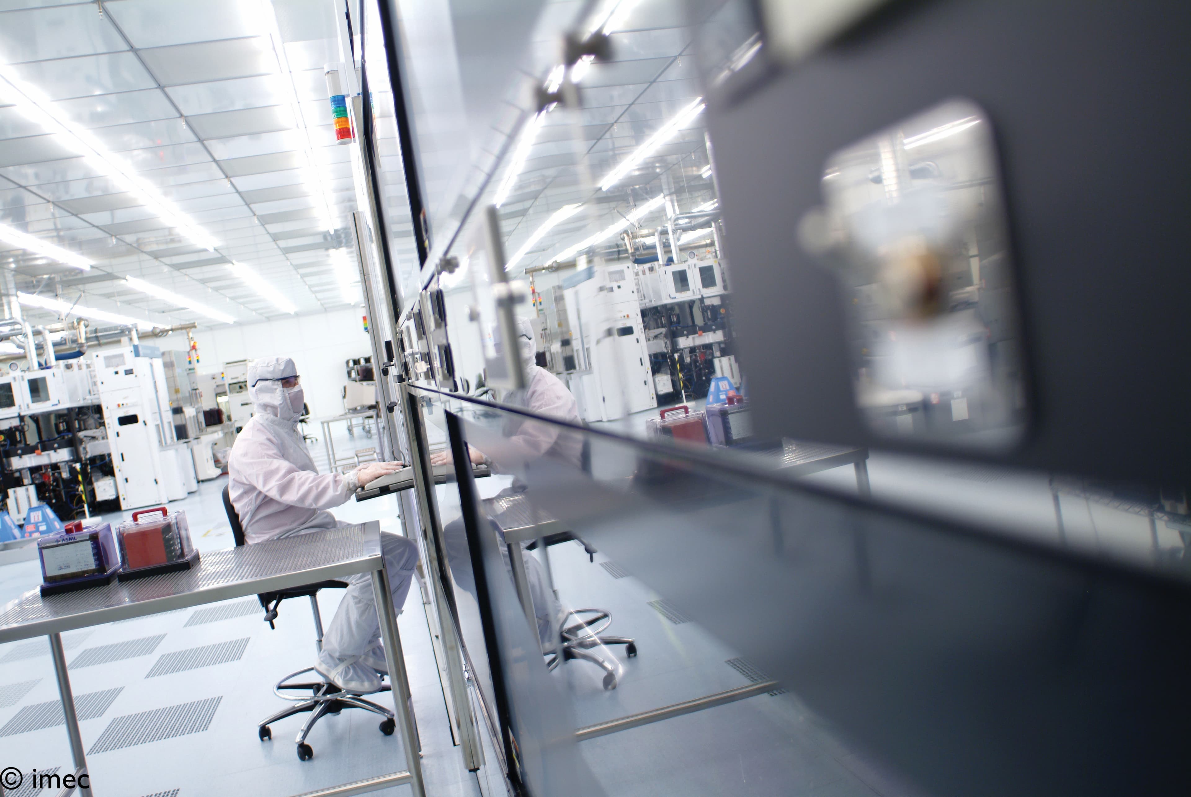
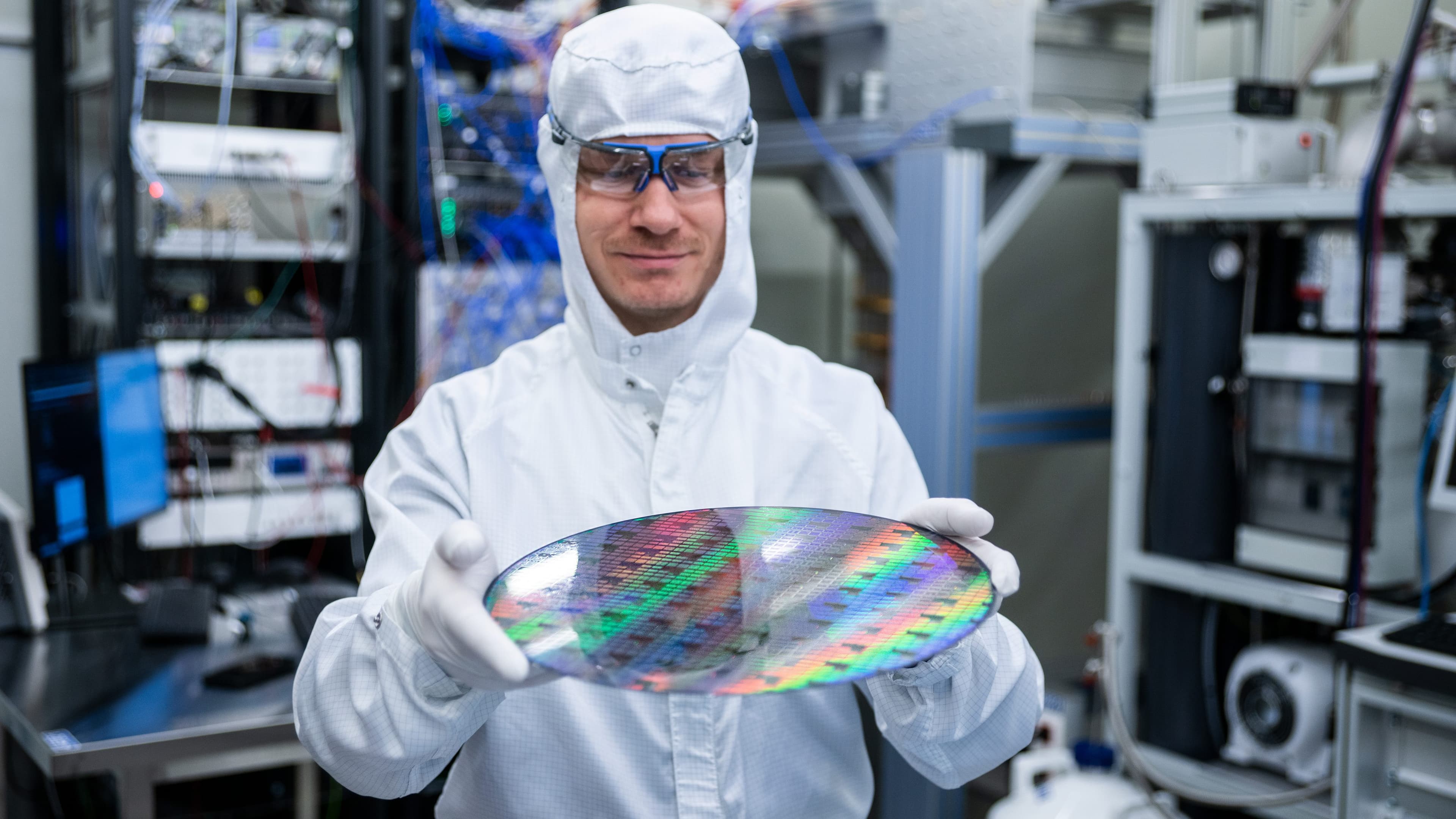
Imec leverages cutting-edge fabrication and state-of-the-art 300mm tooling for advanced semiconductor technology nodes to fabricate qubits at scale with high coherence times, low variability, and high yield.
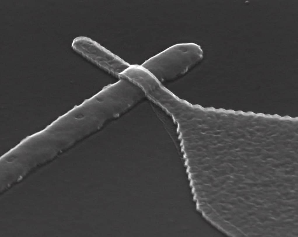
A large part of imec’s activities is devoted to the study of materials, as well as improving the quality of surfaces and interfaces in quantum devices. We utilize advanced test and characterization facilities to study the behavior of a range of materials and processes to identify the most promising options for qubit development.
Spin qubits
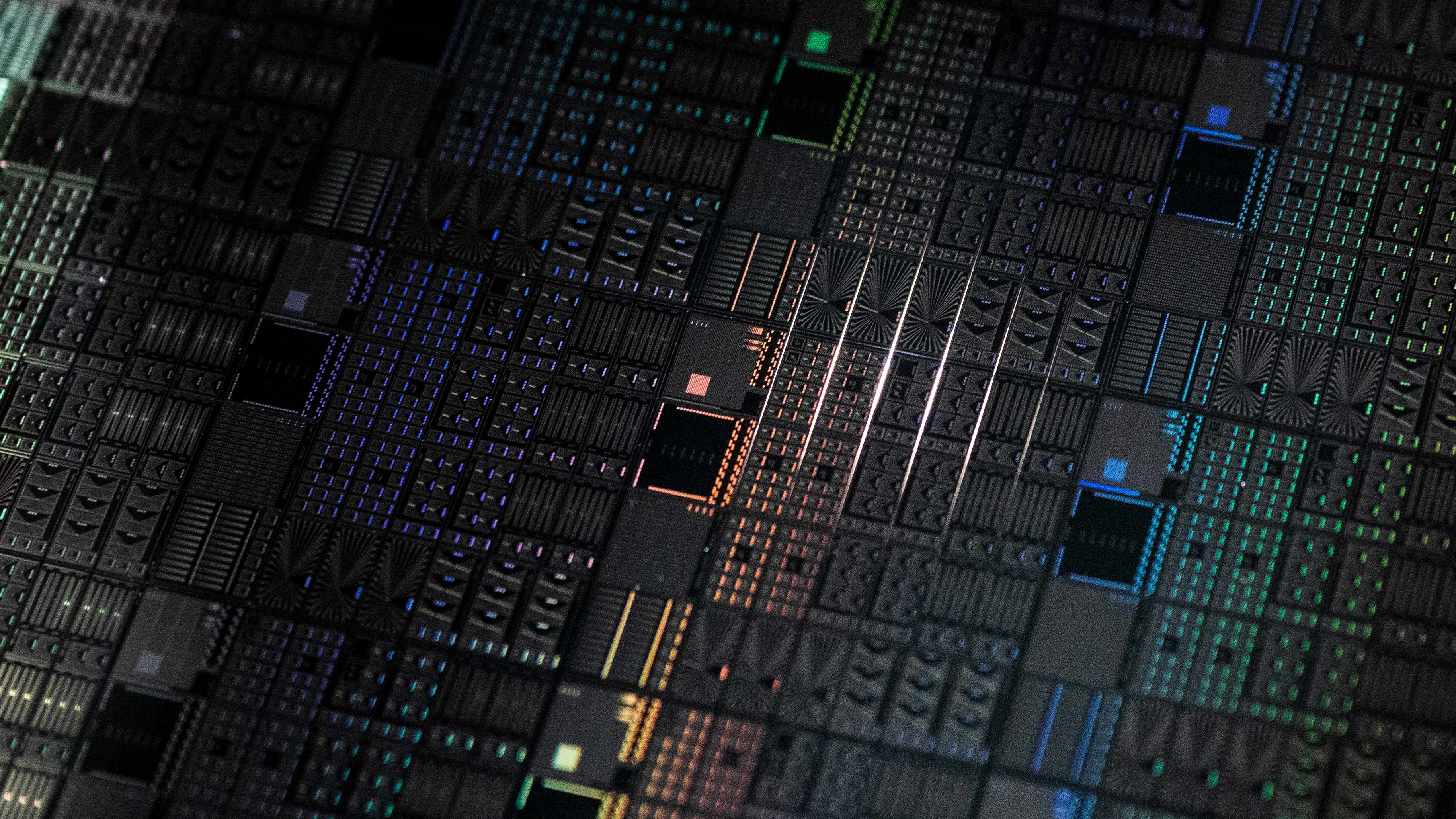
Spin qubit devices highly resemble standard CMOS transistors. We fabricate them on imec’s 300mm industrial fabrication line. The primary goal is to achieve:
- high quantum coherence and low qubit variability
- flexible back-end-of-line integration and control periphery for large-scale qubit arrays
In addition, standard CMOS characterization is coupled with cryogenic device testing towards understanding material properties and improving the process flow. This enables the accurate identification of those factors that limit the performance of qubits in relation to the fabrication process.
2026 press release: Imec presents quantum dot qubit device using High NA EUV lithography
2026 press release: Semiconductor-based quantum pilot line ‘SPINS’ launched with EU support
2026 article: Si MOS quantum dot spin qubits: roads to upscaling
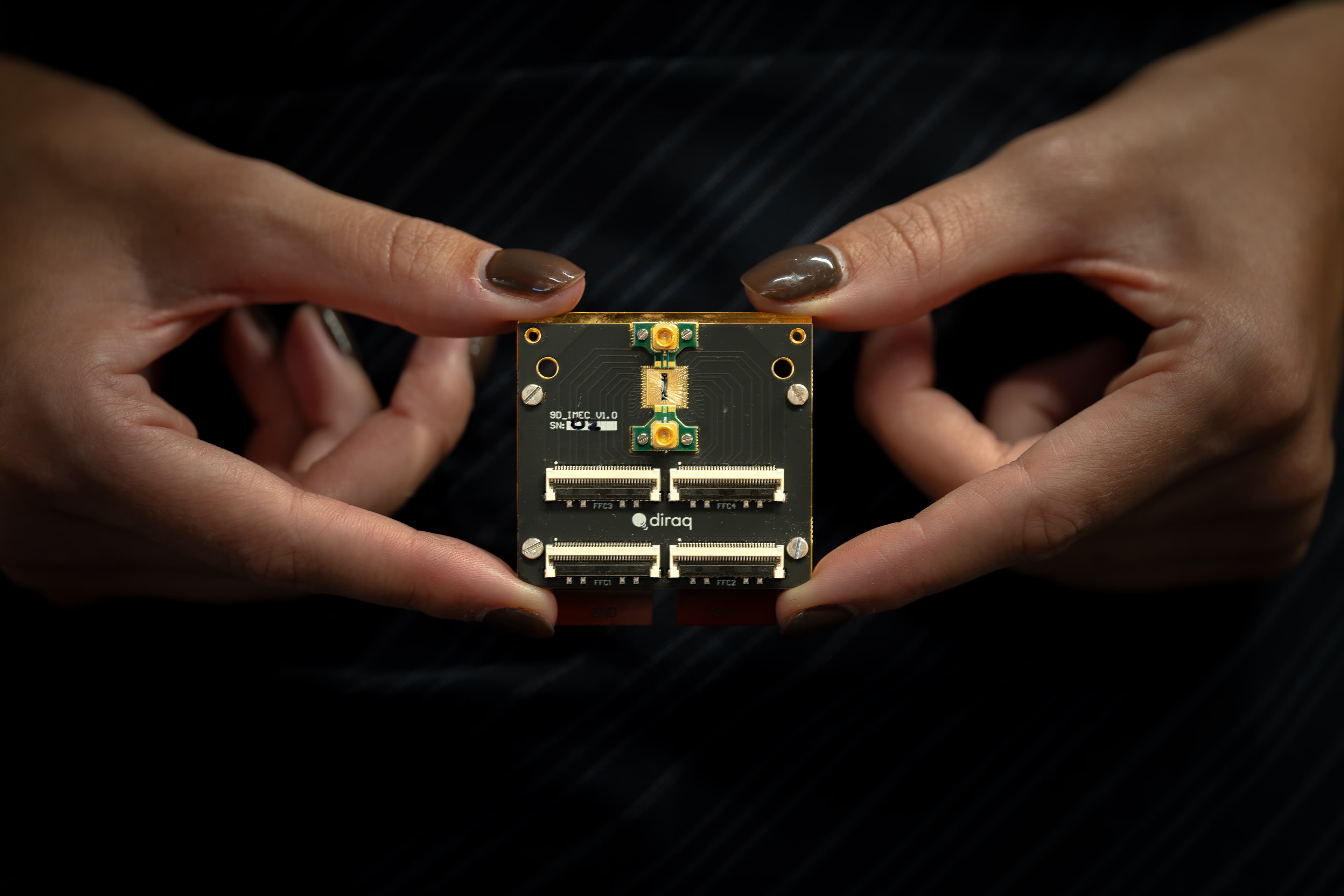
2025 press release: Imec technology lights the path to utility scale for Diraq’s quantum chips

Do you want regular updates on imec’s semiconductor research?
Superconducting qubits
There’s a need for superconducting qubit fabrication techniques that can be fully integrated and are compatible with state-of-the-art 300mm industrial processing, including 3D integration.
Imec’s focus is on achieving high-coherence, low-variability, and high-yield quantum devices. To achieve these goals, we’re fabricating qubits and conducting extensive studies on materials, surfaces, and interfaces. New fabrication techniques are also explored, to ensure high-quality surfaces and interfaces. Those are critical to achieving high-fidelity superconducting qubits.

Cryo 3D integration
Imec's deep expertise in 3D integration on foundry-compatible 300mm platforms can be leveraged for quantum computing. Going to the third dimension can increase the density of qubits while reducing the footprint. It can also help address some of the scalability challenges currently facing qubit development.
With imec's 3D integration capabilities, it may be possible to interface large-scale qubit arrays with a standard industrial fabrication-compatible process.

Cryo CMOS device testing, and modeling
The complexity of future quantum computers could be tamed by dedicated classical supporting electronics. To enable scaling, reduce footprint, and minimize power consumption we’re exploring the behavior of classical CMOS electronics at temperatures down to the millikelvin regime.
We’re performing technology characterization and developing transistor models at cryogenic temperatures. Based on these foundations, we explore novel circuit concepts that can control qubits without degrading their performance.

Work with us
Want to accelerate your own quantum computing activities?
Through a bilateral R&D collaboration, you can leverage imec’s infrastructure and expertise. We offer support with both quantum devices and the periphery.
Imec not only helps you to address technological challenges. Thanks to our thorough knowledge of the industry, we function as your full-fledged strategic partner – right down to venturing support.
Scientific publications
Qubits
Materials
Cryo CMOS
Modeling and simulation
News and views