[NanoIC topic] Ab-initio-NEGF transport in Ultra-thin Si/SiGe/Ge nanosheets
PhD - Leuven | More than two weeks ago
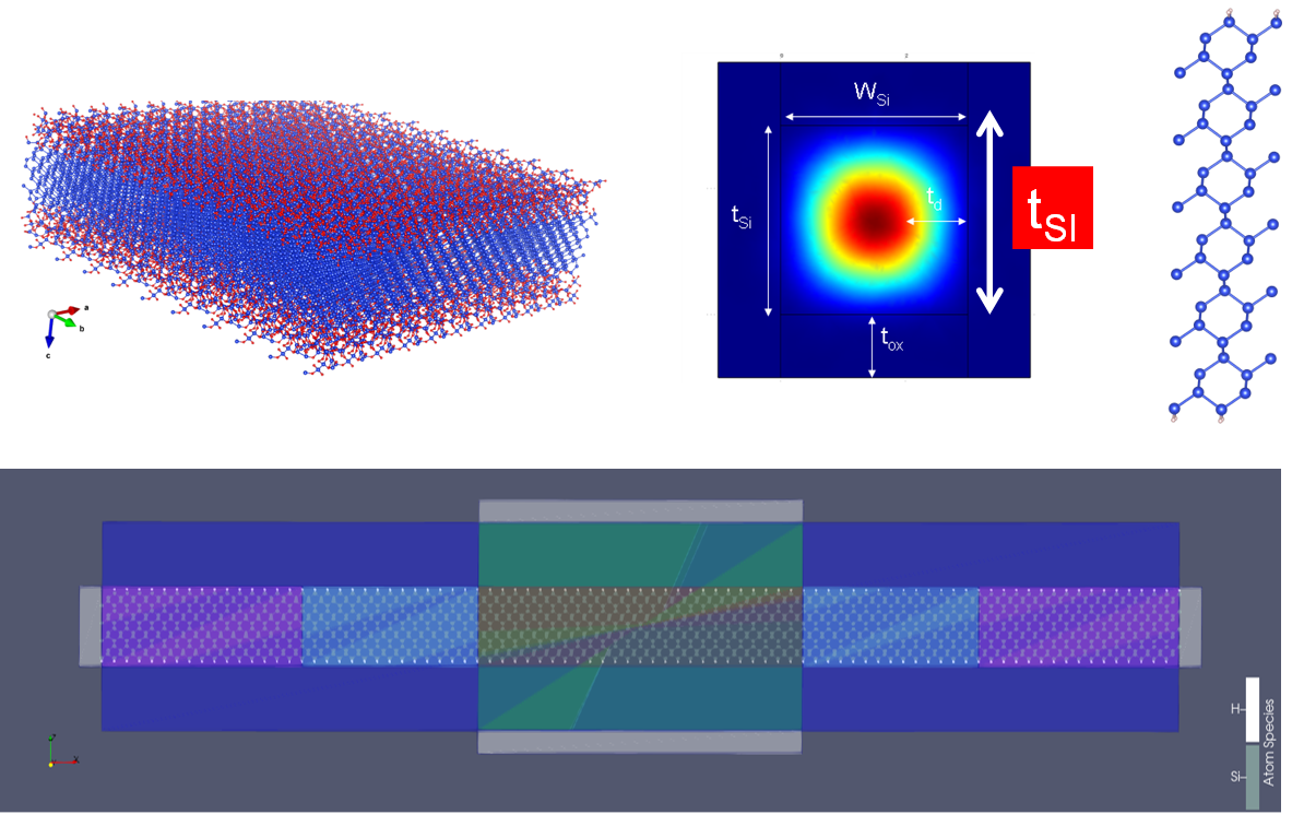
CMOS logic device scaling is approaching the limits of physical scaling due to short channel effects. To maintain electrostatic control of the gate over the channel, the channel thickness also needs to be scaled. While 2D materials such as transition metal dichalcogenides offer an ultimate scaling frontier, integrating these materials into real MOSFET devices presents numerous challenges. Channel scaling of nanosheet transistors made of group IV materials (Si, Ge or SiGe) offer a practical intermediate solution and it is crucial to study and push their scaling limits with extreme body thinning down to 1 nm.
In such aggressively-scaled materials, quantum effects such as extreme quantum confinement (QC), tunneling and atomistic interfaces strongly dominate the electronic properties and transport, so that fundamental understanding of the properties and potential of these materials for device applications are difficult to assess by experiments alone and their modeling requires efficient fully ab-initio atomistic simulation methods, such as Density-Functional-Theory (DFT), combined with quantum transport simulations.
The proposed work relies on the use and possible development of our advanced dissipative ab-initio atomistic Non-Equilibrium Green’s Functions (NEGF) simulator, ATOMOS [1,2,3], combined with state-of-the-art DFT tools (Quantum Espresso, CP2K, PERTURBO, PHONOPY, ...), to explore the fundamental physics, transport properties (including tunneling, electron-phonon interactions, Temperature dependency…) and study the limit of Group IV scaling for nanosheet (NS)/CFET transistors and possibly cryo-CMOS, including material optimization, orientation, Si/Ge grading, thicknesses and device geometry optimization using DFT-NEGF techniques, required for accurate quantification of complex competing effects in ultra-scaled devices. Temperature effects
You will have the opportunity to work in collaboration with a team specialized in atomistic modelling. Since imec is a place where innovation and fundamental research are combined, in a tight bond to applications and industrial partners, you will also be exposed to and closely interact with experimentalists, working on the fabrication and characterization of such devices [4], as well as have interactions with the systems design team when setting up compact models for them calibrated against experimental data. At the same time, your work will support and guide the experimental exploratory programs at imec. Finally, through imec academy, you will have a wide range of training possibilities.
[1] Afzalian, A. Ab initio perspective of ultra-scaled CMOS from 2D-material fundamentals to dynamically doped transistors. npj 2D Mater Appl 5, 5 (2021). https://www.nature.com/articles/s41699-020-00181-1
[2] A. Afzalian, E. Akhoundi G. Gaddemane, R. Duflou and M. Houssa, "Advanced DFT–NEGF Transport Techniques for Novel 2-D Material and Device Exploration Including HfS2/WSe2 van der Waals Heterojunction TFET and WTe2/WS2 Metal/Semiconductor Contact," in IEEE Transactions on Electron Devices, vol. 68, no. 11, pp. 5372-5379, Nov. 2021, doi: 10.1109/TED.2021.3078412 (invited)
[3] A. Afzalian, F. Ducry, Pushing the limits of ab-initio-NEGF transport using efficient dissipative Mode-Space algorithms for realistic simulations of low-dimensional semiconductors including their oxide interfaces, 2023 International Conference on Simulation of Semiconductor Processes and Devices (SISPAD), September 27 – 29, Kobe, Japan, 2023, pp. 305-308. doi: 10.23919/SISPAD57422.2023.10319548
[4] D. Batuk, S. Baudot, T. Schram, E. Rosseel, A. Afzalian, A. Dangol, A. De Keersgieter, A. Vandooren, E. Vecchio, S. Choudhury, B. Chou, N. Horiguchi, P. Heremans, Planar FD-SOI NFETs with Ultra-Thin Si Body: Device Process Integration, SSDM 2025, Sept. 15-28, 2017, Yokohama, Japan
Required background: Physical/Electrical/Electronic/Materials/Nanoscience Engineering, Physics or Chemistry
Type of work: 10% literature review, ~25% DFT simulation of new material, ~50% NEGF device physics and simulations, ~15% code development
Supervisor: Anne Verhulst
Co-supervisor: Aryan Afzalian
Daily advisor: Aryan Afzalian
The reference code for this position is 2026-110. Mention this reference code on your application form.