Chemically-tuned 2D materials for next-generation nanoelectronics using first-principles quantum transport modeling
PhD - Leuven | More than two weeks ago
Two-dimensional (2D) materials, such as layered chalcogenides, are an exciting new class of materials with extraordinary physical and chemical behaviors. They have the potential to enable new technological applications ranging from next generation nanoelectronic transistors to photonics, quantum bits... In particular, as further scaling of Si CMOS transistors is expected to saturate in mid-term future, 2D materials are under investigation as a possible replacement for Si.
To realize this potential and overcome various challenges, for example at their interfaces, the synthesis of novel, high-quality 2D materials, with a broad spectrum of chemical modification techniques, and a thorough understanding of how these modifications control the material physics is highly desirable.
One of the aspects to be studied is doping and defects and their impact on the metal-2D-semiconductor interface. Doping is key in many applications and is not possible by traditional implant techniques in atomistically-thin 2D materials. Doping is paramount in reducing the contact resistivity at the metal-semiconductor junctions present in any transistor. A promising way to achieve doping, in 2D materials, is to locally alter the chemical structure by replacing the transition metal or chalcogenide atom with an atom of a different species to induce in-situ doping or even induce a phase change from semiconducting to metallic. Defects that are naturally present in any materials, e.g., like sulfur vacancies, may further affect the properties of the 2D material and its contact resistance. Defects in the channel, for instance at the oxide/semiconductor interface may also affect the scaling limits of 2D materials and this also needs to be investigated carefully.
Finally, chemical tuning could be used to induce novel properties, such as Janus material and magnetism. The impact of multi-layers with angle or pattern misalignment and their impact on electronic and transport properties could be further studied.
Fundamental understanding of the properties and potential of these materials for device applications are difficult to assess by experiments alone. Ab-initio atomistic methods, such as Density-Functional-Theory (DFT), combined with quantum transport simulations are required to understand the intricate impact of chemical tuning on the electronic and transport physics and properties of 2D materials.
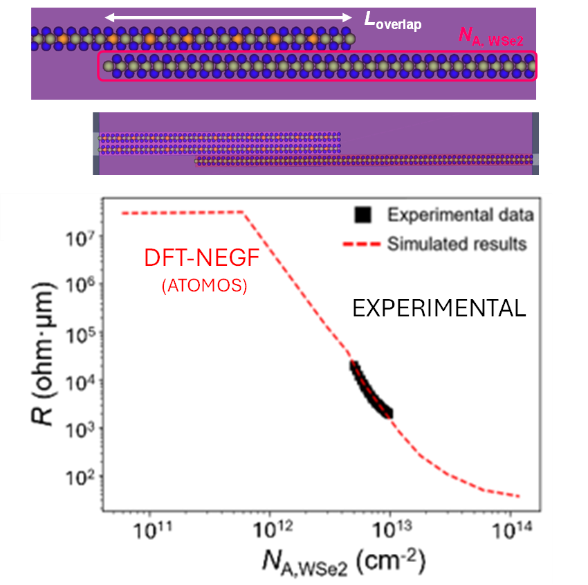
The proposed work relies on the use and possible development of state-of-the-art DFT tools (Quantum Espresso, CP2K...) combined with our advanced dissipative ab-initio atomistic Non-Equilibrium Green’s Functions (NEGF) simulator, ATOMOS [1,2], to explore the fundamental physics, transport properties and application potential for nanoscale devices made of 2D materials, both free-standing and including their interfaces (e.g., metal/semiconductor contact), including chemical tuning, substitutional atoms for doping, vacancies… [3].
You will have the opportunity to work in collaboration with a team specialized in atomistic modelling. Since imec is a place where innovation and fundamental research are combined, in a tight bond to applications and industrial partners, you will also be exposed to and closely interact with experimentalists, working on the fabrication and characterization of such devices, as well as have interactions with the systems design team when setting up compact models for them calibrated against experimental data. At the same time, your work will support and guide the experimental exploratory programs at imec. Finally, through imec academy, you will have a wide range of training possibilities.
[1] Afzalian, A. Ab initio perspective of ultra-scaled CMOS from 2D-material fundamentals to dynamically doped transistors. npj 2D Mater Appl 5, 5 (2021). https://www.nature.com/articles/s41699-020-00181-1
[2] A. Afzalian, E. Akhoundi G. Gaddemane, R. Duflou and M. Houssa, "Advanced DFT–NEGF Transport Techniques for Novel 2-D Material and Device Exploration Including HfS2/WSe2 van der Waals Heterojunction TFET and WTe2/WS2 Metal/Semiconductor Contact," in IEEE Transactions on Electron Devices, vol. 68, no. 11, pp. 5372-5379, Nov. 2021, doi: 10.1109/TED.2021.3078412 (invited)
[3] Duflou, R., Pourtois, G., Houssa, M., Afzalian A. Fundamentals of low-resistive 2D-semiconductor metal contacts: an ab-initio NEGF study. npj 2D Mater Appl 7, 38 (2023). https://doi.org/10.1038/s41699-023-00402-3
Required background: Physical/Electrical/Electronic/Materials/Nanoscience Engineering, Physics or Chemistry
Type of work: 10% literature review, ~25% DFT simulation of new material, ~50% NEGF device physics and simulations, ~15% code development.
Supervisor: Michel Houssa
Co-supervisor: Aryan Afzalian
Daily advisor: Aryan Afzalian
The reference code for this position is 2026-063. Mention this reference code on your application form.