First-Principles investigation of reliability challenges at 2D Material–3D Oxide Interfaces
PhD - Leuven | More than two weeks ago
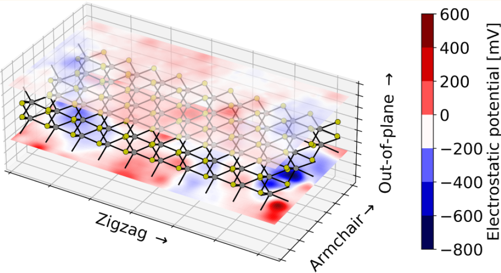
2D materials, such as transition metal dichalcogenides, are promising candidates for the next generation of ultra-scaled transistors. However, their electrical performance in experimental devices still falls short of theoretical predictions: measured carrier mobilities are typically one to two orders of magnitude lower than values obtained from ab initio calculations. Gaining a deeper understanding of the factors limiting carrier mobility—and identifying pathways to mitigate them—is essential to unlocking the full potential of 2D materials in future electronic technologies.
Several mechanisms have been proposed to explain the degradation of carrier mobility in 2D materials, including the effect of dielectric interface inhomogeneity on their electronic properties. Our group has recently investigated this aspect using fully atomistic interface models and found that dielectric inhomogeneity can make a significant contribution to mobility degradation [1,2]. However, that work was limited to pristine 2D materials, whereas in practice these materials typically contain many defects. The goal of this PhD project is therefore to extend the understanding of reliability and transport in 2D materials by:
- Combine Density Functional Theory calculations with non-equilibrium Green's functions to quantify the impact of defects on transport in 2D materials, including the role of the dielectric environment. Extract statistics for different models.
- Develop and implement correction schemes for the spurious interactions between charged defects. Predict the stability of charged defects in 2D materials.
- Correlate with experimental groups at imec to provide theoretical guidance for improving mobility in 2D materials.
- Investigate the role of remote phonon scattering on the 2D materials' mobility.
- Investigate the properties of interfaces between 2D materials and their native oxides.
We are looking for a candidate with a strong drive for understanding things on a deeper level. Some flexibility on the content to include machine learning for example is possible. We aim to provide an environment where the PhD candidate can thrive scientifically and personally, while pushing for technological progress and scientific collaboration internally and externally.
[1] B Van Troeye, F Ducry et al., ACS nano 19, 11664 (2025).
[2] M Dossena, B Van Troeye, npj 2D Materials and Applications 9, 67 (2025).
Required background: Master in Physics, Chemistry or Engineering Sciences
Type of work: 90% modeling and simulation, 10% literature
Supervisor: Bart Partoens
Daily advisor: Benoit Van Troeye, Fabian Ducry
The reference code for this position is 2026-061. Mention this reference code on your application form.