CMOS: advanced and beyond
Discover why imec is the premier R&D center for advanced logic & memory devices.
Integrated photonics
Take a look at technologies for optical transceivers, sensors and more.
Health technologies
See how imec brings the power of chip technology to the world of healthcare.
Sensing and actuation
Explore imec’s CMOS- and photonics-based sensing and actuation systems.
Connectivity technology
Look into our reliable, high-performance, low-power network technologies.
More expertises
Discover all our expertises.
Research
Be the first to reap the benefits of imec’s research by joining one of our programs or starting an exclusive bilateral collaboration.
Development
Build on our expertise for the design, prototyping and low-volume manufacturing of your innovative nanotech components and products.
Venturing and startups
Kick-start your business. Launch or expand your tech company by drawing on the funds and knowhow of imec’s ecosystem of tailored venturing support.
Education and workforce development
Imec supports formal and on-the-job training for a range of careers in semiconductors.
Solutions
Use one of imec’s mature technologies for groundbreaking applications across a multitude of industries such as healthcare, agriculture and Industry 4.0.
Thin films and patterning response in EUV device scaling
Leuven | More than two weeks ago
Explore the impact of material parameters of the thin films stack on EUV lithography patterning response
Extreme Ultraviolet (EUV) lithography stands as a pivotal advancement in semiconductor manufacturing, crucial for sustaining the industry's relentless pursuit of smaller and more powerful chips [1]. EUV lithography utilizes extremely short wavelengths of light, allowing for much finer feature sizes than conventional optical lithography. EUV technology has already enabled the production of cutting-edge processors and memory chips [2]. However, to push the boundaries even further, the industry is transitioning to High-NA EUV lithography [3]. This shift involves increasing the numerical aperture, which effectively enhances the resolution and precision of the lithographic process.
EUV lithography patterning and subsequent etching steps rely on the thin films stack that is used for pattern transfer into the final layer of interest. This stack has been engineered for both lithographic needs, as well as an optimized etch process in terms of selectivity and profile. However, the impact of the properties of this film stack on the patterning outcome are not well characterized or understood. The role of individual film material properties and interactions between layers need to be understood in relation to the outcomes of EUV patterning post lithography and post etch transfer (i.e., critical dimension (CD) control and its uniformity across the wafer, the line-edge roughness (LER) and line-width roughness (LWR), and the defectivity). The fundamental understanding of material properties and their relationship to EUV patterning outcomes will help drive advancements in High-NA innovation.
As part of this PhD work, you will work to define and systematically study the material properties that induce a change in the patterning outcome. You will quantify the impact of surface and bulk material properties on the resulting patterning metrics at lithography and etch levels. You will use advanced semiconductor processing tools in imec’s 300mm clean room, as well as characterization techniques such as Fourier-transform infrared spectroscopy (FTIR), X-ray photoelectron spectroscopy (XPS), X-ray reflectivity (XRR), Time-of-Flight Secondary Ion Mass Spectrometry (TOFSIMS), and Atomic force microscopy (AFM). You will formulate directions on material design toward device scaling and material patterning strategy from a thin films perspective. You will also have the opportunity to work with a team of researchers with vast experience on these topics that will be able to offer guidance and feedback.
[1] M. van de Kerkhof et al., Solid State Electron 155, p20 (2019)
[2] Moore et al, IEEE Spectrum 55-1, p46 (2018)
[3] Levinson et al, Jpn. J. Appl. Phys. 61, SD0803-1 (2022)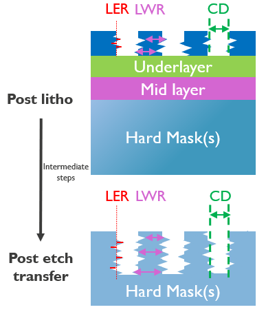
Required background: chemical engineering; materials science and engineering; chemistry; nanoscience & nanotechnology; physics
Type of work: 10% modeling/simulation, 80% experimental, 10% literature
Supervisor: Annelies Delabie
Co-supervisor: Danilo De Simone
Daily advisor: Maria Chistiakova
The reference code for this position is 2024-044. Mention this reference code on your application form.