Unraveling Photoresist Exposure Mechanisms in Extreme Ultraviolet Lithography
Leuven | More than two weeks ago
Leverage advanced processing and materials characterization techniques to elucidate the mechanism responsible for printing the nanosized patterns of integrated circuits.
Micro and nano electronics are the key building blocks that enable the advanced performance of electronic devices that have permeated our everyday lives. These fascinating devices are made ever more powerful and efficient by the continual shrinking of nanoscale transistors that make up their design. This continued scaling has been achieved and maintained over many decades of integrated circuit (IC) manufacturing by incredible advancements in a wide range of technologies that ultimately enable the formation of tiny, nanoscale circuitry patterns. Of these exciting advancements, lithography (in which an optical image is projected and recorded into a photosensitive material, a photoresist) has played one of the biggest roles in enabling the reduction of feature size in nearly all IC components. No matter what nanoelectronic device is used in your daily life (a high-performance CPU in your smartphone, a powerful AI chip, a high-capacity USB drive, etc.), they all share the common foundation of having small components formed by writing optical images in photoresist.
Recently, extreme ultraviolet lithography (EUVL) has entered high volume manufacturing for logic and memory devices and promises to extend the current scaling of size and power of nanoelectronics for years to come. In EUVL, ionizing radiation at a wavelength of 13.5 nm is impinged onto a photoresist to form an image of the desired nanoscale pattern. While the formation of the image in the 13.5 nm light is controlled to an unprecedented degree, the transfer of this image into the photoresist material is determined by a complex interplay of radiation physics and chemistry, with a mechanism mediated by interactions of photons, electrons, and molecules. The complexity of these interactions has made it extremely challenging to uncover the fundamental chemical transformations that are underlying EUVL, which in turn has resulted in an incomplete understanding of the photoresist exposure mechanism. This knowledge gap makes it difficult to engineer designer photoresists that can perform to the highest degree, which will in turn enable the production of ever smaller and powerful electron devices.
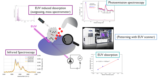
In this PhD project, you will play a pivotal role in helping to bridge the knowledge gap created by an incomplete understanding of the photoresist exposure mechanism. By leveraging advanced fabrication, processing, characterization, and lithographic capabilities at imec, you will perform experiments aimed at uncovering the photoresist exposure mechanism in various model materials, the learnings of which will be directly applied to state-of-the-art materials that form the bedrock of modern EUVL. You will have access to spatial and temporal techniques that utilize and help develop the latest developments in laser-based photoemission, EUV and IR spectroscopy, mass spectrometry, and EUV lithography to perform a holistic investigation, and thus understanding, of the photoresist exposure mechanism. The learnings gained from these mechanistic studies will then be linked to actual patterning performance from an EUVL scanner, providing a crucial missing link for understanding photoresist performance.
Who You Are:
- Master’s degree in engineering, physics, chemistry, materials science, or a related field.
- Motivated, inquisitive student with a passion for learning new concepts and advancing current knowledge bases.
- Prior experience with materials characterization, lithography, optical and ion-based spectroscopy are strong advantages.
- A demonstrated track record of performing experiments and working independently, while also coordinating within a larger team.
- Familiarity with programming languages (Python, MatLab, etc.) and data analysis softwares (e.g., Origin) is a strong plus.
- Excellent written and oral communication in English
What We Provide:
- A diverse, dynamic working environment that employs international experts in nearly every discipline in semiconductors
- An extensive training network covering both technical and non-technical skillsets
- Participation in national/international conferences and workshops
- Fully funded scholarship (with benefits)
Required background: Physics, Chemistry, Materials Engineering and Research, with a focus on spectroscopy and characterization of thin film systems. Prior cleanroom and lithography experience, as well as coding proficiency (Python, Matlab, etc.), are all a plus.
Type of work: 60% experimental, 20% data analysis, 10% modeling/simulation, 10% literature
Supervisor: Pol Van Dorpe
Co-supervisor: John Petersen
Daily advisor: Fabian Holzmeier
The reference code for this position is 2024-175. Mention this reference code on your application form.