
Gallium-nitride power devices
Gallium nitride devices, with their high electron mobility, wide bandgap, and excellent thermal conductivity, are the preferred candidates for power electronics, electric vehicles, the electric grid and renewable energy systems.
Gallium Nitride (GaN) power devices use gallium nitride as semiconductor material instead of the more conventional silicon. Because of their unique properties – high electron mobility, wide bandgap, and excellent thermal conductivity – they offer advantages over traditional silicon-based devices in terms of efficiency, power density, and performance in high-frequency applications.
First introduced as a promising material for high-end PV inverters, GaN has now more widely been adopted by the market, e.g., for mobile phone fast chargers. Thanks to their reliable and successful operation in these applications, the technology will be used more broadly in the future. For example, for power electronics in data centers, electric vehicles and the industrial market.
2026 article: Unlocking the full potential of GaN technology for next-gen power electronics
Performant and reliable GaN power products
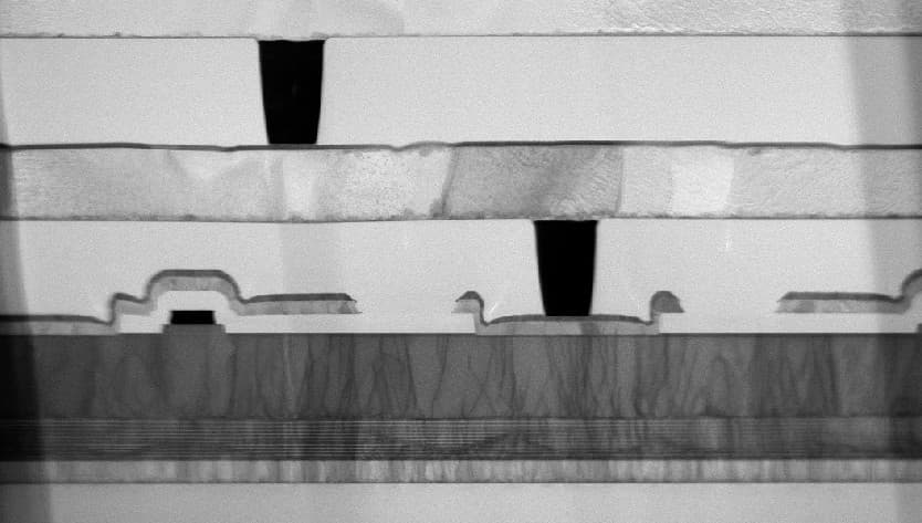
Imec studies how to make GaN devices more reliable and performant by diving deep into device physics, power switching and failure mechanisms. Next to this, imec develops new device concepts for future generations. The devices are made on 200mm silicon, SOI or QST™ substrates and on 300mm wafers. The latter enables the development of more advanced power electronics devices and a reduction of manufacturing costs.
2025 press release: Imec launches 300mm GaN program
These device concepts are available in the 40V to 1200V nodes:
- GaN high-electron-mobilitytransistors (HEMTs). This is one of the most common types of GaN power devices, used in high-frequency and high-power applications, such as smartphone chargers, Class D audio amplifiers, EV on-board chargers, and EV inverters.
- GaN schottky diodes. These devices exhibit faster switching characteristics and lower conduction losses compared to traditional silicon diodes and are typically used in power rectification applications.
- GaN Power ICs integrate multiple GaN power devices and control circuitry on a single chip. They are used in various power electronic applications, including power supplies, motor drives, and converters.
Research update: monolithic integration of GaN components boosts power integrated circuits
You can work with imec on this topic in various ways, depending on your needs:
- Do you want imec as your R&D partner, to complement and empower your GaN team? Step into imec’s IIAP program. This gives you insights into emerging technologies (such as lateral p-GaN HEMTs and vertical GaN FETs) and technological trends, and early access to advanced GaN power devices.
- Do you want to shorten your time to market? Ask imec for a technology license or transfer. Two mature platforms are available: 40V/100V p-GaN HEMT and 200V/650V p-GaN HEMT, both with monolithic integration (GaN-IC) possibilities.
- Do you want to design your device with imec’s GaN technology? Our multi-project wafers are available to this end.
- Do you want to tune our device technology towards your needs? Our team can guide you in a dedicated development project.
Imec also develops GaN technology and devices for RF applications.
Want to work with us? Let us know what you are interested in and how we can help.
Click the button below to get in touch.


Subscribe to our thematic newsletters