
The emerging role of AI in advancing the lithography and patterning ecosystem
Advances in lithography and patterning have been fundamental to the continued dimensional scaling of logic and memory devices. Over the years, imec, ASML, and its ecosystem of partners achieved continuing progress by pursuing a holistic co-optimization approach, in which design, materials, lithography processes, masks, optical proximity correction (OPC), metrology and inspection, are optimized simultaneously.
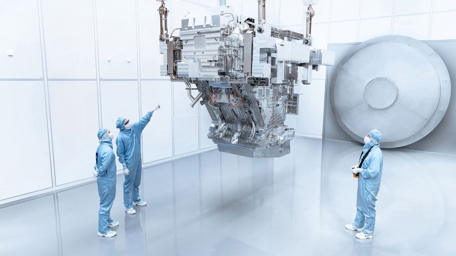
The resolution of the optical lithography system could advance by utilizing either a smaller wavelength of light (e.g., the transition from 193nm DUV to 13.5nm EUV light) or by increasing the numerical aperture (NA) of the lithography system. The latter approach marked the transition from 193nm dry to 193nm immersion lithography. More recently, this same principle has underpinned the development of High NA (0.55 NA) EUV lithography, enabling imec to guide the industry into the ångström era. While these optical adjustments repeatedly improved the resolution of the aerial images, continuous innovations in all other aspects of the ecosystem were needed to fully unlock the capabilities of advanced lithography.
More recently, the advent of AI and the expanding scope of GPU-based accelerated computing (AC) have created significant opportunities to accelerate key developments across the lithography and patterning ecosystem. This led imec and NVIDIA to collaborate. As part of the collaboration, NVIDIA develops AI and AC solutions, leveraging imec’s leading position in litho and patterning R&D.
In this article, the collaboration is illustrated with two specific use cases. The first focuses on the AI-driven de-noising of CD-SEM metrology, leveraging the tremendous capabilities of AI in boosting image processing. The second demonstrates how NVIDIA’s cuLitho library, a CUDA-X library for GPU-accelerated computational lithography, has delivered the performance gains required for computationally intensive process-window OPC (PW-OPC) workloads.
Use case 1: AI-based de-noising algorithm to support sub-1nm CD-SEM metrology
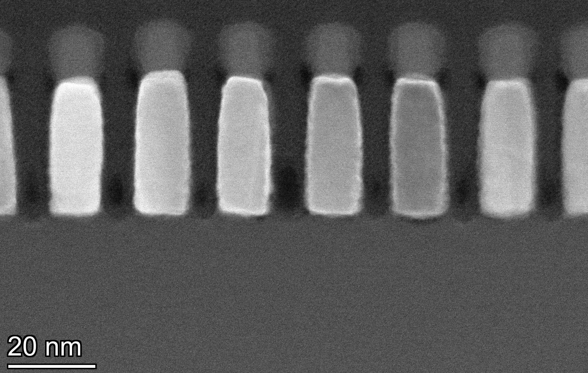
Throughout the history of Moore’s Law, device dimensions have scaled more rapidly than metrology resolution has improved. This limitation is particularly pronounced in CD-SEM metrology, the industry-standard technique for measuring key metrics of patterned features, such as critical dimension (CD) and line-width roughness (LWR).
As lithography systems transitioned to shorter exposure wavelengths or higher numerical apertures to print smaller features, thinner photoresist layers became necessary to mitigate pattern collapse. The need for thinner resists became even more critical with the advent of High NA EUV lithography, helping to account for the reduced depth of focus (DOF) inherent to operation at higher NA.
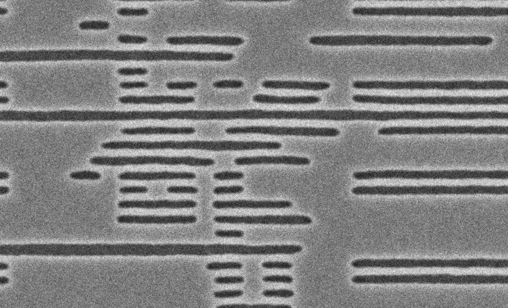
The reduced resist thickness, however, lowers the secondary electron emission from the topography, resulting in reduced signal-to-noise ratio (SNR) of the SEM images – significantly degrading image contrast. And this deteriorates the accuracy of CD and LWR measurements, contributing to an overall metrology error. It is, however, essential to accurately measure parameters like CD in order to maintain the quality of nm-scale devices, especially when there is an expected statistical variation in feature size and shape.
In the frame of their collaboration, imec and NVIDIA started using AI/deep learning to address the shortcoming in resolution provided by state-of-the-art CD-SEM techniques. While imec contributed with measured CD-SEM data and validation experiments (using best-known methodologies), the NVIDIA team developed a generative adversarial network (GAN)-based deep learning methodology for de-noising CD-SEM data.
By using this de-noising methodology, the SNR of a single CD-SEM data frame (or raster scan) could be significantly improved, on average, by 5.5x. This resulted in a much-improved accuracy of CD and LWR measurements, mainly supporting sub-nm metrology for High NA EUV lithography. The developed AI methodology has been validated using power spectral density (PSD) analysis of the AI-reconstructed images. It has also proven to be applicable to a broad range of imaging conditions, involving, for example, various resist and underlayer combinations.
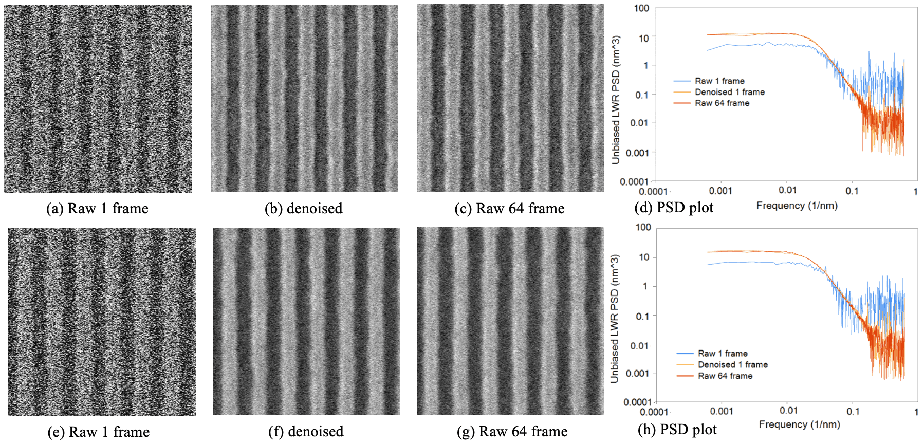
Figure 1 – Illustration of applying the de-noising algorithm for two different process conditions. (b) and (f) show the denoised 1-frame images that are presented in (a) and (e); (c) and (g) display the raw 64-frame images for comparison; (d) and (h) present PSD graphs used to assess the quality of the de-noised images. [Source: M. Kim et al. (2023)."Frequency-informed deep-learning denoising method supporting sub-nm metrology for high NA EUV lithography", DTCO and Computational Patterning II. CD-SEM image by imec and AI generated image by NVIDIA.]
Other, more conventional approaches typically average an increasing number of frames (up to 64) to generate high-SNR images, each frame (or scan) adding to the data acquisition time. Compared to these frame-averaging approaches, the proposed de-noising methodology largely improves wafer throughput (with up to a factor of 64) as it uses only one single ‘noisy’ frame as input.
“Imec’s advanced R&D has enabled us to identify critical technology bottlenecks that could not be resolved using conventional techniques. By combining imec’s lithography and patterning expertise with NVIDIA’s leading AI and AC technologies, we can now overcome these barriers and accelerate lithographic progress in dimensional scaling, including the High NA EUV era.” – Ryoung-Han Kim, R&D Director at imec
Use case 2: AI and GPU-accelerated computing to improve process-window OPC
With continued advances in lithography and patterning, computational lithography techniques such as optical proximity correction (OPC) have become essential for maintaining pattern fidelity at wafer level at increasingly scaled dimensions. Without OPC, the patterns transferred onto the silicon wafer do not precisely reproduce the shapes of the intended circuit layout. This is due to the light experiencing diffraction when propagating through the lithography scanner and mask, as well as to physical and chemical effects in the photosensitive layer. If left uncorrected, printed structures appear with irregularities such as line widths that are narrower or wider than designed, or corners being rounded. Minimizing errors from design to wafer necessitates the use of OPC techniques that correct the pattern before it is written onto the mask.
Conventional OPC techniques change the mask shapes based on nominal lithography conditions such as the optimal focus condition of the scanner (i.e., zero focus) and nominal exposure dose. More recently, the OPC community started considering process-window OPC (PW-OPC), which takes into account multiple process variations including out-of-focus and changing dose conditions. Such an approach would allow better predictability of real wafer shapes in a broader set of process conditions. This is particularly important for High NA EUV lithography, which suffers from a reduced DOF compared to 0.33NA lithography.
Conventional CPU-based computational resources can however not handle the workload required by PW-OPC. The latter is not only too computationally heavy, but it also requires expanding the optimization domain to include multiple dimensions.
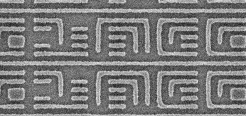
The collaborative work between imec and NVIDIA shows that AI-based methods and GPU-accelerated computing can help addressing this computational bottleneck. Expanding OPC with AI and GPU-based computational lithography techniques in NVIDIA’s cuLitho library has resulted in a 30% improved process window, as measured on wafers with 3nm layouts for M0 and M2 metal lines. This directly impacts the yield of the lithographic process and supports an increase in DOF – which is particularly useful for High NA EUV lithography.
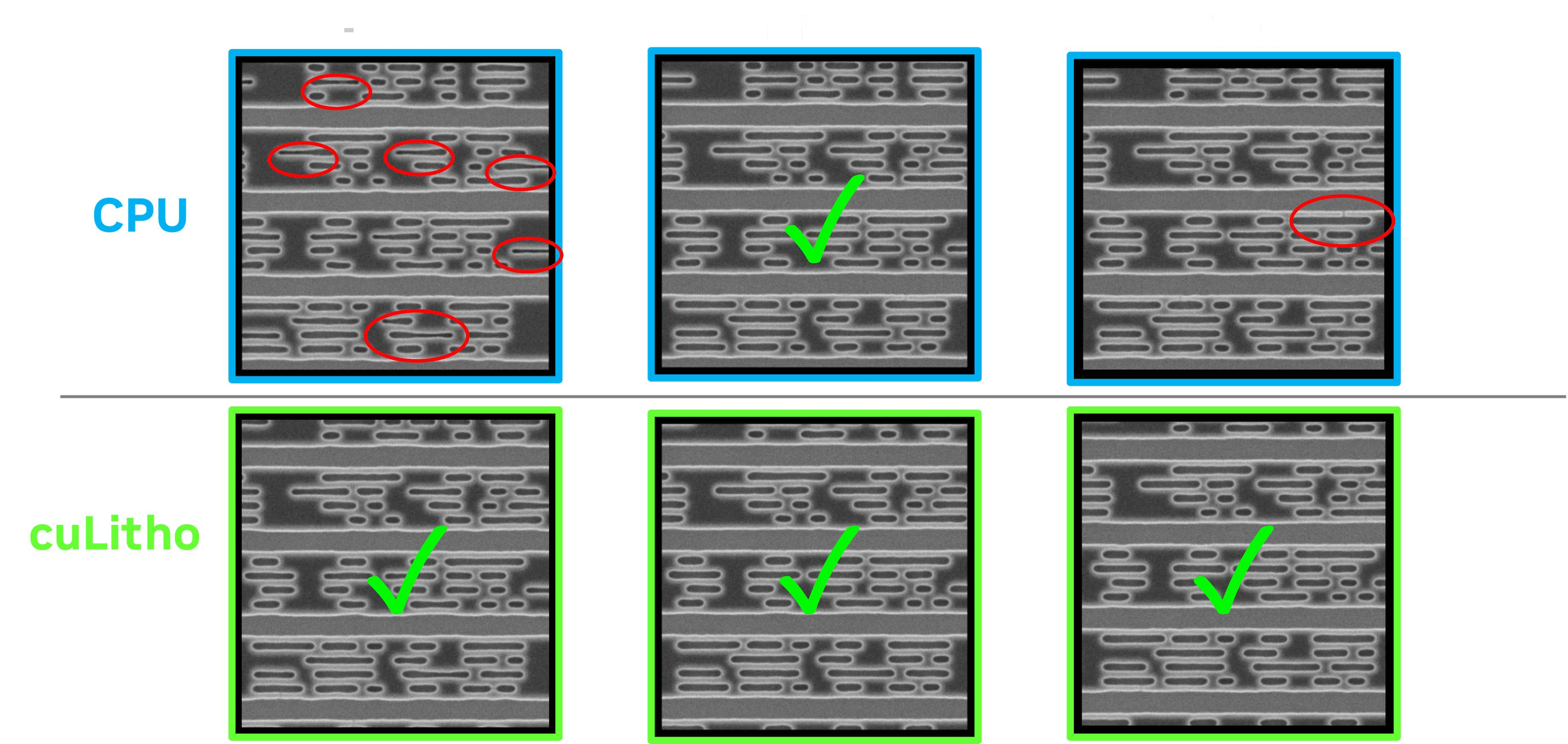
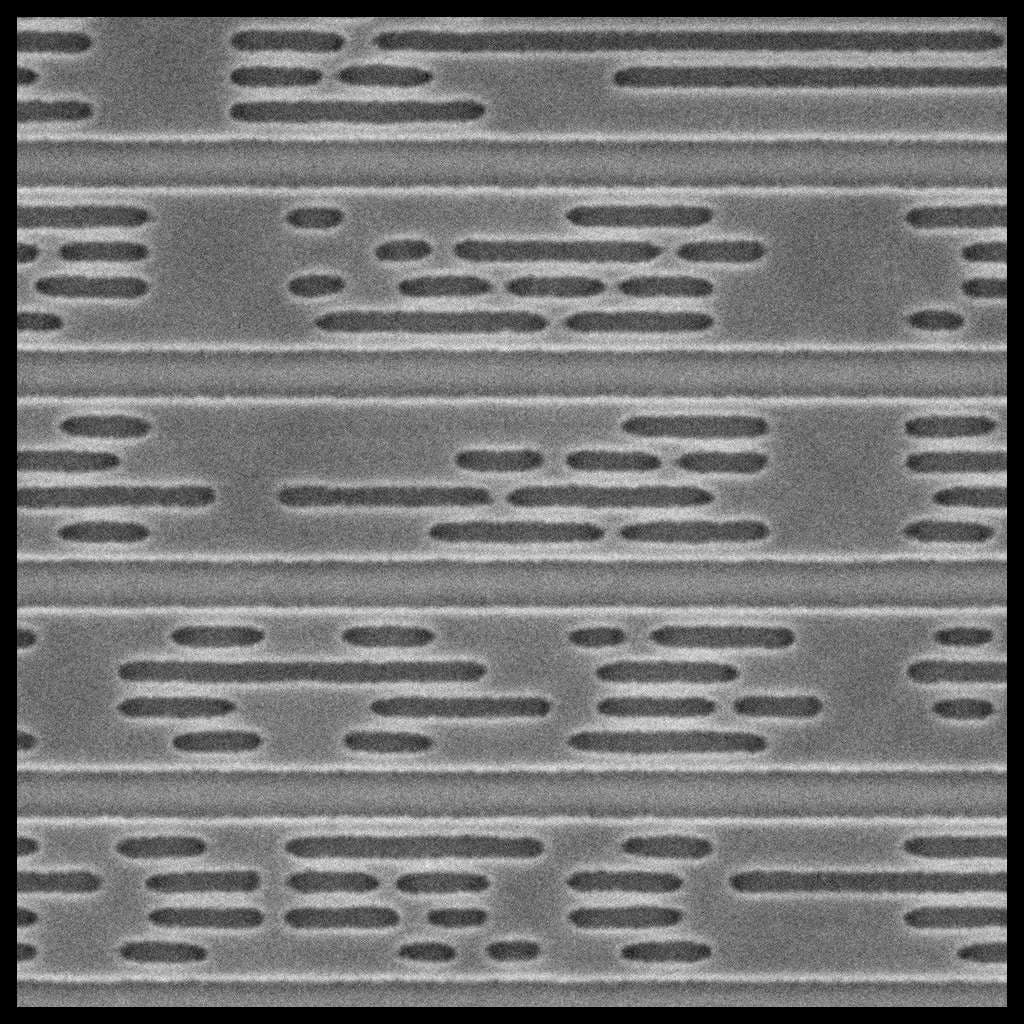
Figure 2 – Process-window OPC improvement obtained using AI and GPU-accelerated computing. The results are obtained on wafers with 3nm layouts for M0 and M2 metal lines. [Source: V. Singh (2025), "The future of computing is accelerated”, imec ITF World 2025 Keynote.]
Conclusion
AI and AC have already been shown to drive substantial advances across the semiconductor industry, including in lithography and patterning. The imec-NVIDIA collaboration demonstrates how these computational technologies can address long-standing technical challenges associated with continued dimensional scaling in two examples; de-noising CD-SEM images for improved measurement accuracy; and enabling process-window OPC for enhancing DOF and yield. The availability of these AI-based methods will particularly be useful for accelerating the development of next-generation High NA EUV lithography and patterning.
Imec and NVIDIA are broadening the scope of their collaboration, further exploring the capabilities of NVIDIA’s AI and AC engines in enhancing the efficiencies for lithography and semiconductor technology.