Press release
Imec Achieves Record Low Contact Resistivity on Ga-doped Ge Source/Drain Contacts for pMOS Transistors
LEUVEN, Belgium—Dec. 4, 2017 – At this week’s 2017 International Electron Devices Meeting (IEDM), imec, the world-leading research and innovation hub in nanoelectronics and digital technology, reports ultralow contact resistivity of 5x10⁻¹⁰Ωcm2 on Gallium (Ga)-doped p-Germanium (Ge) source/drain contacts. The low contact resistivity and high level of Ga activation were achieved after nanosecond laser activation (NLA) at low thermal budget. The results show that highly Ga-doped Ge-rich source/drain contacts provide a promising route for suppressing parasitic source/drain resistance in advanced pMOS devices.
These breakthrough results are important in light of further downscaling of the CMOS source/drain contact area, which is challenged by a parasitic source/drain resistance and results in suboptimal transistor functioning. High dopant activation is known to be an attractive approach for lowering source/drain contact resistance. Traditionally in pMOS devices, Silicon (Si) source/drain contacts with high boron (B) activation are used. But in more advanced pMOS devices, Ge- and SiGe(Sn)-based source/drain are a promising alternative since they introduce beneficial strain. However, the higher the Ge content, the lower the boron activation and solubility in Ge or Ge-rich SiGe.
The new findings result from a comprehensive study of Ga dopant activation in Si, Si0.4Ge0.6 and Ge conducted by imec, KU Leuven (Belgium) and Fudan University (Shangai, China). In this study, either rapid thermal annealing (RTA) or Applied Materials’ nanosecond laser activation (NLA) were used as dopant activation technologies, after Ga ion implantation. A record low contact resistivity of 5x10⁻¹⁰Ωcm2 and a high dopant activation level of 5x1020cm-3 were obtained for Ga-doped Ge source/drain contacts after NLA. The low contact resistivity can be attributed to a beneficial Ge/Ga surface aggregation following the NLA process. With RTA activation at 400°C, a contact resistivity as low as 1.2x10⁻⁹Ωcm2 was reported. The study shows that Ga might be preferred over B as a dopant for Ge or high-Ge content source/drain contacts in pMOS devices.
“For the first time, we have achieved contact resistivities far below 10-9Ωcm2 for high-Ge content source/drain contacts,” said Naoto Horiguchi, distinguished member of the technical staff at imec. “This proves that Ga doping and activation by NLA or RTA are an attractive alternative to boron doping for these source/drain contacts. It provides a possible path for further performance improvement using the current source/drain schemes in next-generation technology nodes.”
The results were obtained at low thermal budget activation, making Ga doping particularly attractive for devices that require low-thermal budget processing.
Imec’s research into advanced logic scaling is performed in cooperation with key CMOS program partners including GlobalFoundries, Huawei, Intel, Micron, Qualcomm, Samsung, SK Hynix, SanDisk/Western Digital, Sony Semiconductor Solutions, TOSHIBA Memory and TSMC.
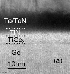
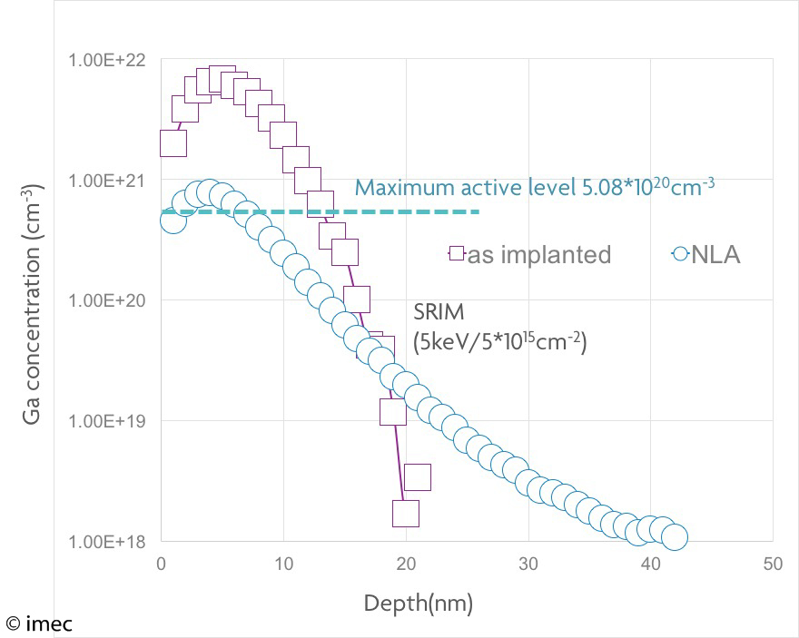
Figure: Ga implanted in Ge and activated by NLA: (left) TEM image and (right) SIMS profile and calculated active carrier concentration level.
About imec
Imec is the world-leading research and innovation hub in nanoelectronics and digital technologies. The combination of our widely acclaimed leadership in microchip technology and profound software and ICT expertise is what makes us unique. By leveraging our world-class infrastructure and local and global ecosystem of partners across a multitude of industries, we create groundbreaking innovation in application domains such as healthcare, smart cities and mobility, logistics and manufacturing, energy and education.
As a trusted partner for companies, start-ups and universities we bring together close to 3,500 brilliant minds from over 70 nationalities. Imec is headquartered in Leuven, Belgium and has distributed R&D groups at a number of Flemish universities, in the Netherlands, Taiwan, USA, China, and offices in India and Japan. In 2016, imec's revenue (P&L) totaled 496 million euro. Further information on imec can be found at www.imec-int.com.
Imec is a registered trademark for the activities of IMEC International (a legal entity set up under Belgian law as a "stichting van openbaar nut”), imec Belgium (IMEC vzw supported by the Flemish Government), imec the Netherlands (Stichting IMEC Nederland, part of Holst Centre which is supported by the Dutch Government), imec Taiwan (IMEC Taiwan Co.) and imec China (IMEC Microelectronics (Shanghai) Co. Ltd.) and imec India (Imec India Private Limited), imec Florida (IMEC USA nanoelectronics design center).
Contact
Hanne Degans, press communications manager, +32 16 28 17 69 // +32 486 06 51 75 // Hanne.Degans@imec.be