
A compact 8-bit, 8GS/s time-interleaved SAR-based analog-to-digital converter (ADC)
High-speed analog-to-digital converters with a 7 to 8-bit resolution are a key component of the radio equipment embedded in next-generation broadband communication devices. Unfortunately, ADCs’ power consumption significantly increases as we tap into higher frequencies. This, in turn, is likely to become a major issue for battery-powered (6G) smartphones.
Using time-interleaved (TI) SAR (successive approximation) ADCs has been an important first step to making ADCs more power-efficient. On the downside, however, they suffer from limited speed due to their underlying sequential conversion mechanism.
Consequently, imec researchers have implemented speed-enhancing techniques in a compact single-bit, single-comparator SAR loop. Their design translates into an impressive 1 giga-samples per second (GS/s) per channel, with a limited signal-to-noise distortion ratio (SNDR) degradation.
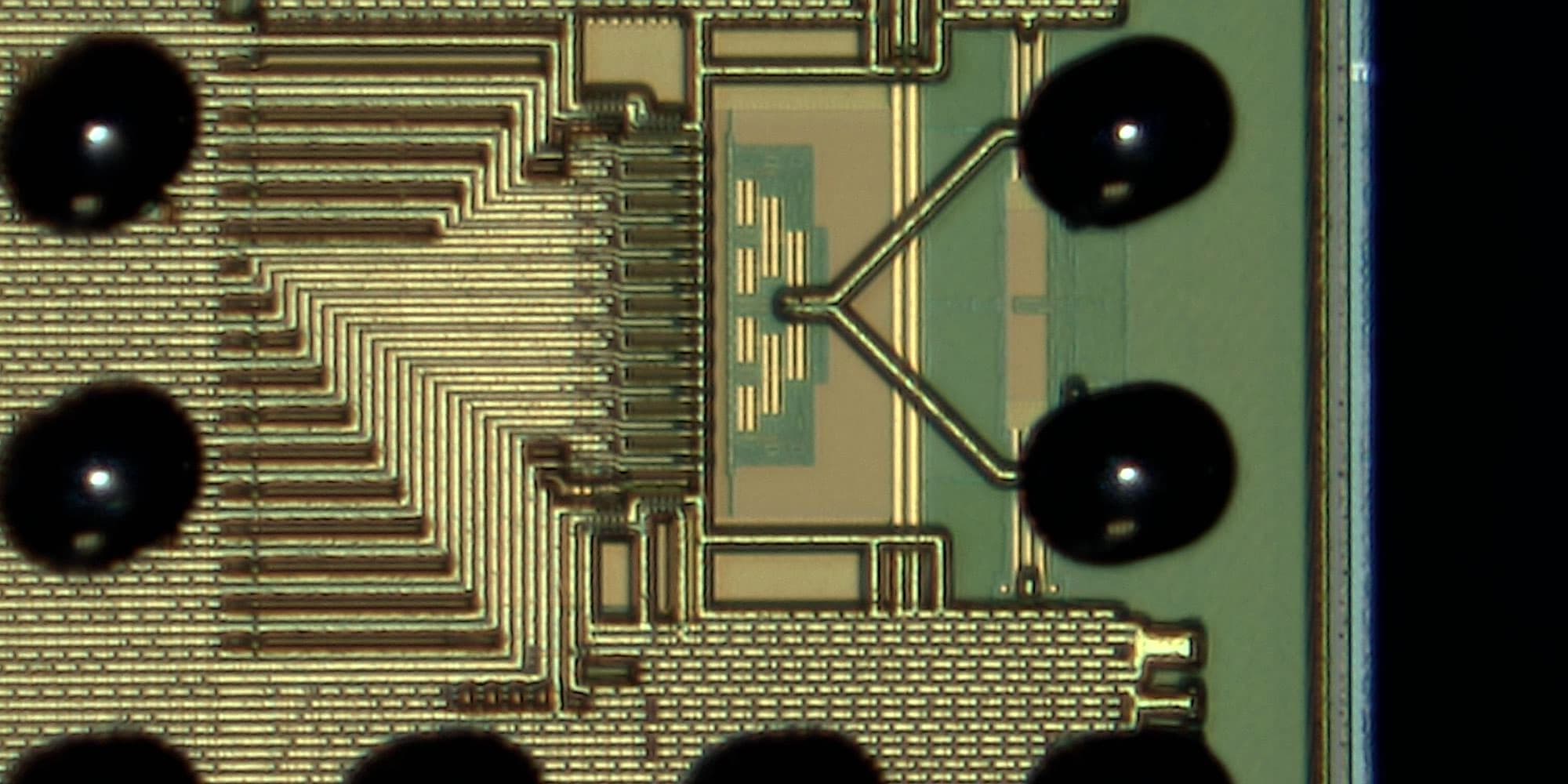
Joris Van Driessche: “Our 8-bit, 8GS/s TI SAR ADC – fabricated in a 16nm CMOS process and with an active area of 210x110µm² – has shown to consume a mere 26mW. That is significantly lower than the energy consumption reported by competitive TI SAR approaches. And it achieves a 45dB SNDR with 1GS/s channels. We think this contribution will be instrumental in developing the next generations of high-speed broadband radio transceivers that come with acceptable power consumption levels.”
A 140GHz transmit/receive (T/R) front-end module (FEM) in 22nm FD-SOI CMOS
The first radio band identified to accommodate beyond-5G services is the D-band – which ranges between 110 and 170GHz. However, it is far from obvious to use standard silicon (CMOS-based) technologies at those higher frequencies due to their limited transmit power and power efficiency.
“Yet, imec’s new 140GHz front-end module is a nice proof point of how silicon technology can still be leveraged to build competitive phased arrays for short-range beyond-5G applications,” highlights Joris Van Driessche. “Thanks to its integrated switch functionality, the same antenna array can be used for the transmit and receive (T/R) modes in a time-division duplex (TDD) communication system. Integrating such a T/R in advanced silicon technology typically comes with significant losses in output power and efficiency. However, by introducing a new topology that avoids using a dedicated switch in the transmit path, we have been able to reduce those losses considerably.”
“Concretely, our compact D-band FEM with integrated T/R switch functionality achieves a saturated output power Psat of 12.5dBm, and a peak-power added efficiency of 11% in transmit mode. In receive mode, it achieves a 9.2dB noise figure for the receiver with a mere 20mW power consumption from a 0.8V supply,” he adds.
What’s next: a research pipeline filled to the brim
As a next step, these components will find their way into a new RF module telecom vendors will be able to experiment with. Estimated time of arrival: end of 2022.
And there is yet more to come, as imec researchers have started to explore a hybrid III-V/CMOS approach to enable medium to long-range applications at frequencies over 100GHz too.
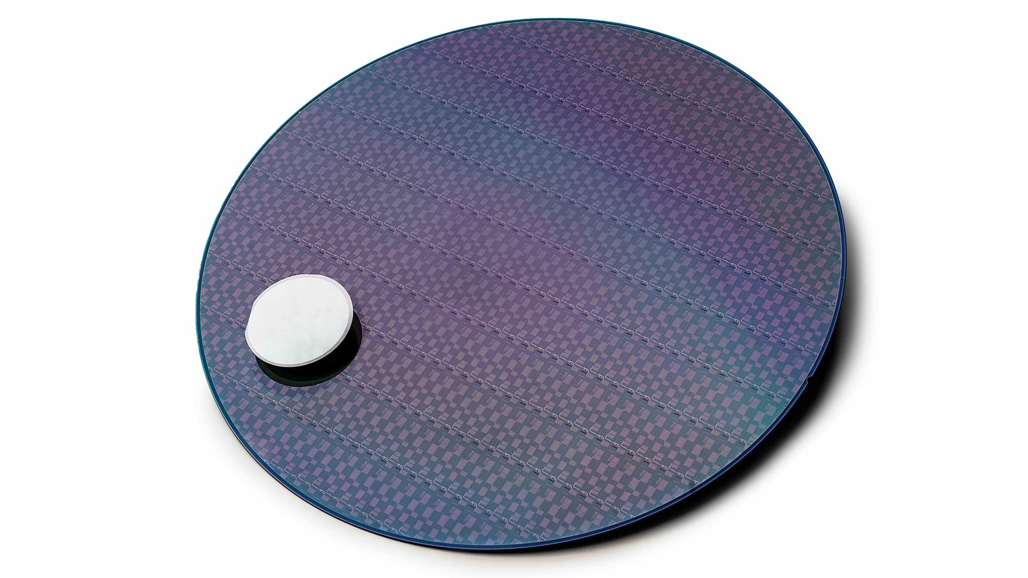
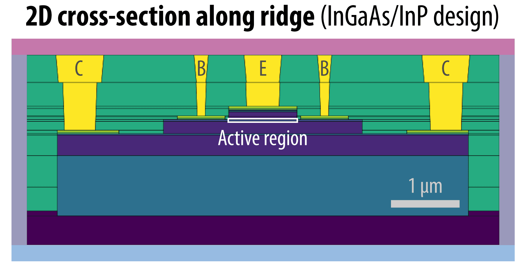
“Here as well, we aim to reduce next-generation radios’ power consumption and footprint significantly. The problem we are facing is that III/V materials – such as indium phosphide (InP) – only come in small wafers, making them less suited for mass-market consumer applications. In addition, they typically have a limited BEOL, which hampers the implementation of complex circuits. And they tend to come with a lower yield too. As part of imec’s Advanced RF program, we try to overcome these limitations, while investigating how III-V materials can heterogeneously be combined with CMOS technology to create mobile device technology that efficiently and cost-effectively operates at 100GHz and beyond,” Van Driessche concludes.
This article previously appeared on the website of Microwaves & RF.

Joris Van Driessche received the M.Sc. degree in Electrical Engineering from Ghent University (Belgium) in 2001. He joined imec in 2001 as an RF front-end architecture research engineer, focusing on system specification and architecture definition for multi-standard RF transceivers.
In 2006, he became project manager for reconfigurable RF transceivers, addressing challenges towards true software-defined radio transceivers optimized for advanced CMOS technologies. He subsequently took on the role of program manager for imec's Advanced RF research program, focusing on millimeter-wave and sub-THz RFICs, antennas, packaging, and system design.
Today, Joris serves as portfolio director, Advanced RF technologies at imec.
Published on:
14 February 2022