The semiconductor industry is evolving at breakneck speed. Artificial intelligence (AI) applications, such as agentic and physical AI, push compute demands to unprecedented heights, forcing a fundamental rethink of system architectures. But while the technology powering this AI revolution has surged ahead, academic research in computing architecture has struggled to keep pace. Until now.
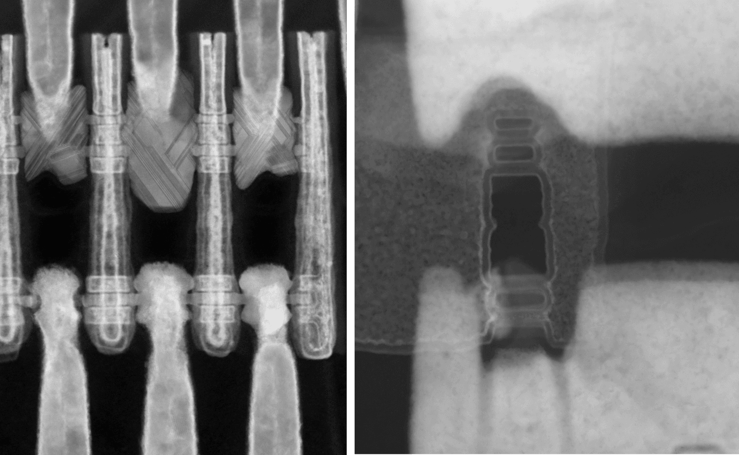
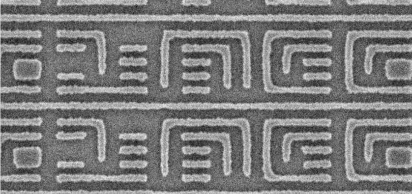
Europe’s NanoIC pilot line, a pioneering European initiative, hosted by imec, is changing the game with its introduction of Pathfinding Process Design Kits (P-PDKs), advanced toolkits that are re-establishing the critical bridge between academic innovation and industrial relevance.
“Historically, universities could conduct meaningful and relevant research at higher levels of abstraction, without detailed access to the underlying technology,” explains Professor Mehdi Tahoori from the Karlsruhe Institute of Technology (KIT). “But with the shift to advanced semiconductor technology nodes, where DTCO (Design-Technology Co-Optimization) and STCO (System-Technology Co-Optimization) are essential, conducting impactful research in computing architectures without direct access to technology has become nearly impossible. As a result, academic research has gradually drifted away from the realities of industrial practice. That’s why the NanoIC pilot line is so important: by providing access to pathfinding PDKs, it bridges the gap between academia and industry.”
The race beyond 2nm semiconductor innovation
We are currently living through a digital revolution. One defined by the rise of artificial intelligence and breakthroughs in sectors such as autonomous driving, healthcare, and industrial automation. For decades, progress was fueled by CMOS scaling, with each new generation of transistor miniaturization delivering faster, cheaper, and more energy-efficient chips.
From the 20-nanometer node onward, this scaling process was further enhanced by additional scaling booster, introducing advanced device architectures such as FinFETs, nanosheets, Forksheets, CFETs, and novel integration solutions such as 3D stacking and chiplet integration. These shifts transformed chip design into a process of Design-Technology Co-Optimization (DTCO) and even System-Technology Co-Optimization (STCO).
But as industry raced towards these Angstrom nodes, where we’re no longer just shrinking transistors, but rewriting the chip architecture, academic research gradually fell behind. When the complexity of semiconductor design increased, traditional abstraction layers, which had long enabled universities to explore realistic design scenarios, no longer matched the complexity of advanced technologies. As a result, university research gradually drifted away from industrial practice, cutting academic researchers off from driving innovation.
That’s about to change with Nano IC’s Pathfinding Process Design Kits (P-PDKs).
Pathfinding PDKs: putting academia back into the semiconductor fast lane
At its core, a Process Design Kit (PDK) is a software environment that enables circuit designers to simulate, validate, and optimize chip designs using realistic models of chip technology. Consider it a blueprint and a simulation toolkit allowing chip designers to explore performance, power, and manufacturability of a new chip architecture in a virtual sandbox.
What sets Pathfinding-PDKs (P-PDKs) apart is that they anticipate future technologies. They’re built on predictive models of upcoming technologies. This allows researchers to explore system-level trade-offs, assess architectural implications, and prepare design flows before the technology reaches maturity, giving innovators, including university researchers, a crucial head start in designing for the next wave of chips.
“When it comes to beyond-2nm semiconductor innovation, you can’t tape out a physical circuit, because the technology simply doesn’t exist yet,” Anita Farokhnejad, DTCO Program Manager at imec, explains. “But you can already explore what the performance will look like, what the system implications are and how to prepare architecture and design flows for what’s coming.”
To support this forward-looking exploration, NanoIC’s P-PDKs are grounded in imec’s 2nm process flows. From this, detailed 3D device structures are modeled and abstracted into compact models for circuit-level simulation. These enable full standard cell libraries, along with predictive transistor models, interconnect stack definitions, parasitic parameters, design rule files (DRC, LVS), and reference design examples. The result: access to a complete design environment and a feedback loop that connects design insights back to technology development.
Accelerating a next-generation semiconductor ecosystem
With the first P-PDK released in 2024 (2nm), and the second coming up in November 2025, access to the P-PDKs is about more than providing early-stage design kits. By serving as a bridge between process innovation and system design, the NanoIC pilot line ensures that the future of compute isn’t shaped behind closed doors but developed in an ecosystem that includes the academic minds best equipped to explore bold new design paradigms.
Professor Mehdi Tahoori: “Universities are ideally positioned to drive out-of-the-box innovation and invent new paradigms for computing. This is where universities shine. But to do that, they need access to the latest technologies and tools. That’s where the NanoIC pilot line is a game-changer: by providing pathfinding PDKs on cutting-edge nodes, it enables academic teams to upskill themselves and work alongside industry to address the pressing challenges of tomorrow’s compute applications. Additionally, it provides a reference technology and platform to benchmark and validate these innovations within a next-generation design roadmap.”
The introduction of Pathfinding PDKs is therefore more than a technical advance. It restores alignment between academic research and industrial practice. Universities can now align their exploration of bold new architectures with advanced technology benchmarks, while industry benefits from disruptive ideas developed in close connection to realistic technology paths.
As such, by enabling early access to predictive design environments and fostering collaboration across academic institutions, research centers, start-ups and industry, NanoIC is laying the foundation for a resilient semiconductor ecosystem, one that has the ambition to continue to accelerate for decades to come.
This article appeared earlier in Power Electronics News
Want to know more?
Interested in exploring the NanoIC ecosystem further? Or discovering the potential sub-2nm roadmap extension being enabled by the Pathfinding PDKs? Make sure to have a look at the NanoIC website.
Interested in using the Pathfinding PDKs for your research or design work? The NanoIC Pathfinding PDKs can be accessed for free via Europractice, a consortium of research organizations that provides European industry and academia with resources to develop electronic circuits and systems.

Anita Farokhnejad earned her PhD from Universitat Rovira i Virgili (Spain), specializing in FEOL and device modelling. She joined imec in 2021 as an R&D Engineer, focusing on BEOL optimization and future roadmap development. Collaborating closely with integration and physical design teams, she develops models for PnR data analysis and BEOL optimization. Her recent work on the enhanced Ring Oscillator (eRO) model aids in the early assessment of new materials and BEOL boosters. In August 2023, she advanced to team lead for PDK Enablement, translating advanced semiconductor nodes into Pathfinding-PDKs. Anita is also dedicated to education, conducting courses that make sophisticated technological concepts accessible to both industry veterans and aspiring engineers. Currently, she serves as Program Manager of DTCO at imec, where her contributions continue to drive innovation in the semiconductor industry.

Mehdi B. Tahoori is Professor and Chair of Dependable Nano-Computing at the Karlsruhe Institute of Technology (KIT), Germany, and guest professor at imec, focusing on CMOS 2.0 and future chip technologies. He previously worked at Xilinx (USA), Fujitsu Labs (USA), and served as a junior professor at Boston Northeastern University (USA) and as a visiting professor at the University of Tokyo (Japan). He earned his B.S. from Sharif University (Iran) and M.S./Ph.D. from Stanford (USA). Prof. Tahoori is Deputy Editor-in-Chief of IEEE Design and Test Magazine, is a former Editor-in-Chief of Elsevier Microelectronic Reliability and has chaired major IEEE symposia. His honors include multiple best paper nominations and conference awards, the US National Science Foundation Early Faculty Development (CAREER) Award (2008), an ERC Advanced Grant (2022), and an IEEE fellowship.
Published on:
24 October 2025


