In just a few years, AI has advanced at a breathtaking pace. The rapid evolution and adoption of ChatGPT (and other LLM-based applications) illustrates this perfectly: what began as a research experiment less than a decade ago is now deeply embedded in everyday life.
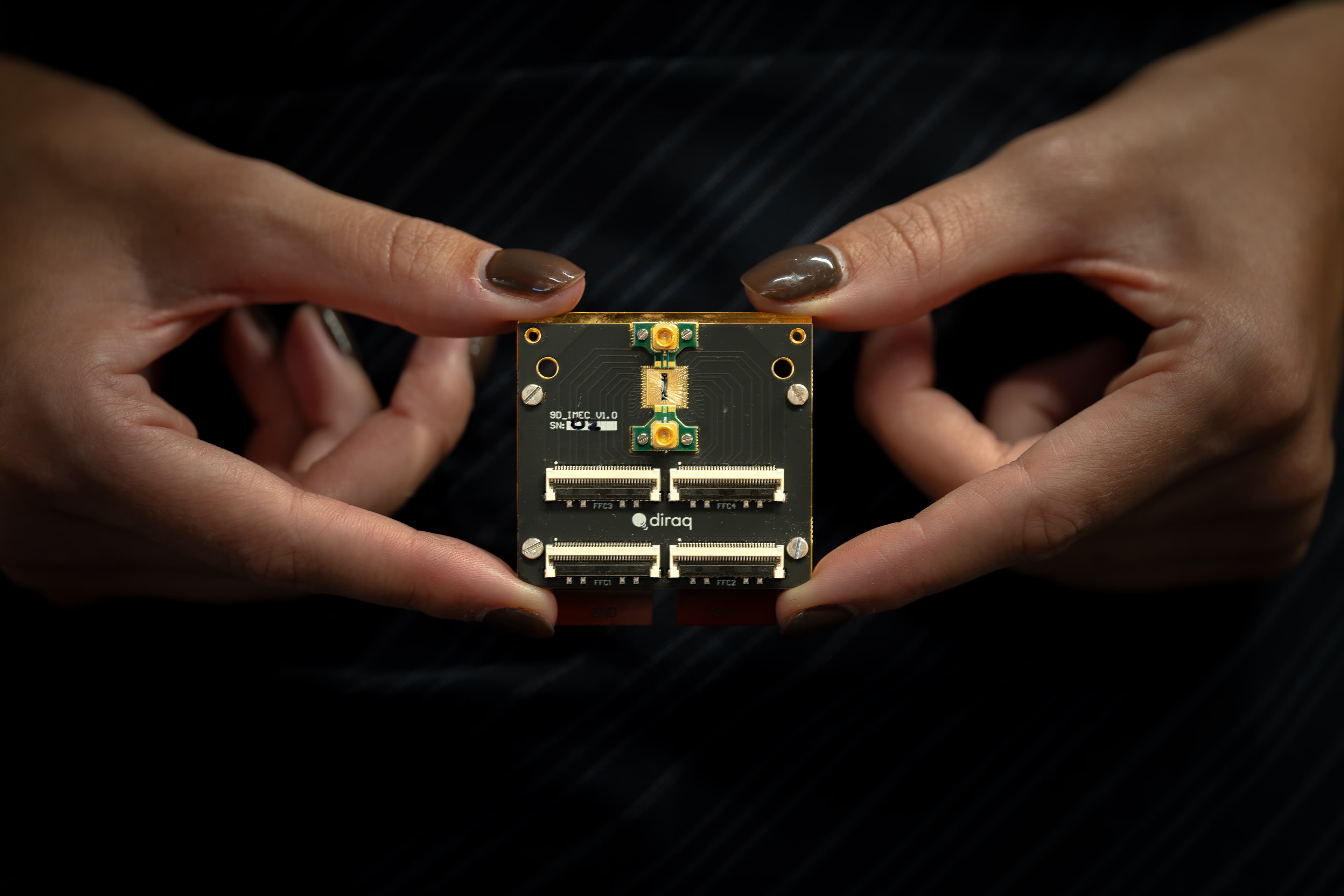
And AI’s momentum is only accelerating. Agentic AI, for example, promises to move beyond generating text or images toward autonomous, context-aware decision-making. Physical AI is next, poised to step out of the digital realm and into the real world, enabling robots, autonomous systems, and other smart devices that can sense, act, and learn.
Agentic and physical AI will change everything
These breakthroughs, however, don’t happen in isolation. Every step in AI is matched by an equally critical evolution in chip technology. In fact, one could say that AI and microchips share a tightly interconnected – almost symbiotic – relationship: advanced semiconductors have been key to the rise of AI, while AI itself now drives demand for ever smaller, more energy-efficient, and increasingly powerful nodes.
Yet, this relationship is under strain. AI models evolve at lightning speed, while chip development remains a multi-year process of design, validation, and production. The result? A widening gap that makes today’s approach – building a new chip for every emerging AI flavor – unsustainable.
According to imec CEO Luc Van den hove and CEO-elect Patrick Vandenameele, these forces will shape not only imec’s next chapter, but the future of the semiconductor industry at large. In this preview, they outline imec’s 2026 strategy for tackling the underlying challenges – and for seizing the opportunities that come with them:
- From cementing imec as a credible and influential AI brand,
- And tackling ever more intricate chip-scaling hurdles through imec’s cross-technology co-optimization (XTCO) paradigm,
- To further maturing High NA EUV lithography,
- Developing the photonics roadmap for sustainable (AI) computing,
- And ensuring that imec’s innovations translate into real market impact.
Positioning imec for the post-LLM era
“The pace at which AI has permeated virtually every aspect of society has been nothing short of mind-blowing. Yet, unlike the semiconductor roadmap – guided for decades by the cadence of Moore’s Law – AI’s trajectory remains far less predictable,” begins Luc Van den hove, CEO of imec.
“Let's take large language models (LLMs) as an example. While they could still play a role in enabling future AI breakthroughs, they come with a significant limitation: they don’t truly learn – they are trained. I believe the next generations of AI – agentic AI, physical AI, and others – will be driven by machine learning approaches such as reinforcement learning, continual learning, and autotelic learning.”
“These learning approaches will enable AI systems to build internal world models – rather than rely on pre-trained language models – and to adapt to new situations without forgetting what they’ve already mastered, much like humans do. Think of how babies learn: through exploration, setting small goals, and satisfying their innate curiosity about how the world works. That kind of agility – guided by self-motivated learning, and an eagerness to self-improve – is exactly what we need to unlock the next leap in AI,” he adds.
“A new era of grand chip scaling challenges has begun.”
Integrating such capabilities into AI systems will inevitably reshape the underlying chip architectures, even if the exact implications are not yet fully understood. But according to imec’s CEO, this uncertainty shouldn’t paralyze the industry. On the contrary, it challenges the semiconductor ecosystem to think boldly about what comes next – and beyond. Imec, for its part, has already begun to make a decisive move in the AI domain.
“2026 will be a pivotal year for imec, a unique moment to continue to position ourselves as a credible and influential AI brand,” says Van den hove. “Ambitious? Certainly. But the opportunity is real. It’s why we have established imec.AI-labs: a team that will connect emerging AI paradigms with our deep semiconductor know-how. Building this lean, highly agile group of a few dozen experts – capable of moving fast and delivering meaningful impact – will be a major priority next year. It will be essential to cement imec as a leading force shaping AI’s long-term roadmap, and by extension, the hardware roadmap for sustainable compute systems.”
Scaling across – and beyond – boundaries with imec’s XTCO paradigm
While imec aims to leapfrog in the AI domain, advancing the underlying chip architectures remains a top priority for 2026 too. This ambition is at the core of all imec research programs. It drives not only innovations in materials and (process) technologies, but also the continued refinement of classic DTCO (design-technology co-optimization) and STCO (system-technology co-optimization) approaches, alongside the introduction of imec's new cross-technology co-optimization (XTCO) paradigm.
CEO-elect Patrick Vandenameele highlights XTCO’s unique value: “Next-generation AI systems are becoming increasingly complex. To meet their demanding memory, power, thermal, and reliability requirements, chips are evolving into heterogeneous assemblies of multiple technologies that continuously interact with – and influence – one another.
“XTCO tackles the challenges that keep our system and fabless partners awake at night – by introducing a disruptive, holistic approach to scaling.”
“The thing is: within this heterogeneity lies an enormous opportunity to optimize and scale across technologies. That is the essence of XTCO. It tackles the challenges that keep our system and fabless partners awake at night by introducing a disruptive, holistic approach to scaling – from compute density, memory capacity and bandwidth, and power delivery and management, to thermal performance, and reliability. We believe meaningful progress can only be achieved by jointly optimizing these dimensions.”
“A new era of grand chip scaling challenges has begun. XTCO is our answer to those challenges,” he adds.
But doesn’t solving a bottleneck in one area risk shifting the limitation elsewhere?
“Absolutely,” Vandenameele acknowledges. “That’s precisely why cross-technology scaling requires constant iteration and dialogue across domains. It’s also why imec is uniquely positioned to lead this effort: our ecosystem brings together all relevant players – enabling the continuous, end-to-end collaboration essential for XTCO to succeed.”
“But make no mistake: materials and (process) technology innovations, from introducing CFET device architectures to taking the next steps in the CMOS 2.0 roadmap – and bringing these innovations from lab to fab – will remain fundamental. This is where enablers such as High NA EUV, 3D integration technology, and photonics come into play.”
Breaking through the silicon ceiling
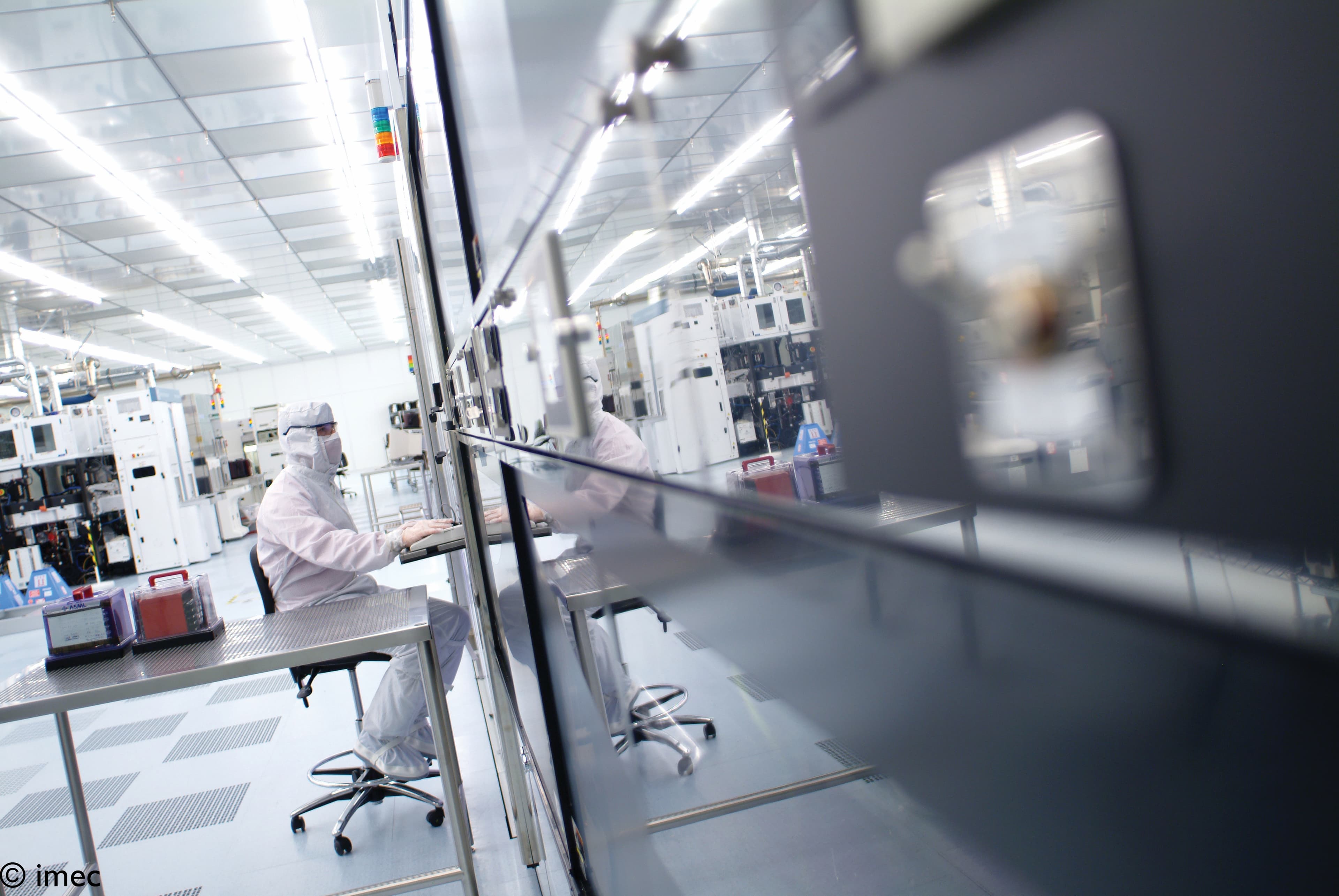
High NA EUV lithography – the next major leap in patterning, enabling sub-2nm chip fabrication – was developed at record pace in the joint ASML-imec High NA EUV Lithography Lab in Veldhoven, the Netherlands.
“Building trust in – and de-risking – new technologies is where imec has always played a critical role. Working closely with our partners, our mission is to mitigate risks and ensure a smooth path to adoption. That’s precisely what we have been doing at the Veldhoven lab,” says Luc Van den hove. “Established to accelerate High NA EUV’s commercial readiness, the lab has delivered extensive data and key breakthroughs – not just in single exposure, but also in patterning advanced logic and DRAM structures – demonstrating that the technology can fully support A10 nodes.”
“2026 is shaping up to be an exciting year for imec, with the next-generation High NA EUV scanner set to be installed on our Leuven campus.”
So, what’s next for High NA EUV – and what role will imec play going forward?
Luc Van den hove: “From an infrastructure standpoint, 2026 is shaping up to be an exciting year for imec, with the next-generation High NA EUV scanner set to be installed on our Leuven campus. Securing this scanner – along with a full suite of state-of-the-art ASML tools – and building the underlying expertise in Europe is a major achievement. It was made possible through support from ASML, the Flemish government, and the EU Chips Act. I cannot stress this enough: investments like these are hard to overvalue. They act as a powerful magnet, confirming and strengthening imec’s position as home to the world’s largest patterning ecosystem, with more than 60 partners. Everyone who matters in lithography and patterning is here.”
“On the research side, our focus remains on helping customers unlock the full potential of High NA EUV – by integrating and testing it in commercial process flows and ensuring platform stability under real manufacturing conditions. At the same time, we will continue to push the limits of High NA EUV by exploring next-generation nodes – including logic A7 and A5, as well as DRAM 0a and DRAM 0b technology.”
“By enabling ultrafast data exchange over short-reach and short-haul interconnects, photonics will form the backbone of large-scale, energy-efficient computing systems – essential for cloud computing and advanced AI workloads.”
“That being said, while a key part of our role is to accelerate High NA EUV’s maturity and ecosystem adoption, we will also continue to advance complementary technologies such as Low NA EUV and immersion lithography – which will remain critical technology options for the creation of less demanding chip layers. Our ongoing cleanroom expansion directly supports that mission,” he adds.
Photonics is emerging as another cornerstone technology – notably when it comes to enabling next-generation computing. By enabling ultrafast data exchange over short-reach and short-haul interconnects, it will form the backbone of large-scale, energy-efficient computing systems. This is essential for cloud computing and advanced AI workloads, which generate massive data flows and demand ultra-high-speed, low-power optical links – both within and between data centers.
Luc Van den hove: “AI has pushed chip scaling and interconnectivity into uncharted territory. The late Dr. Gordon Moore, co-founder of Intel, once proposed that building large systems from smaller, individually packaged, and interconnected components could be more cost-effective. That vision has guided the shift from monolithic chips and 3D integration to massively interconnected chiplet-based systems – where photonics plays a pivotal role. In 2026, imec will continue to lead in this domain, advancing photonic integrated circuits, co-packaged optics, and scalable interconnect solutions to sustain performance growth while managing power consumption and system complexity.”
Venturing into impact
“Our ability to push – and surpass – technological boundaries is what imec is known for. But alongside that exploration effort, there’s another question we must keep front and center: how do we ensure that our innovations reach industry, where they can become the foundation of new products and services? That’s something I care about deeply. Innovation cannot remain confined to imec’s labs and cleanrooms,” says Patrick Vandenameele.
“At the two ends of our innovation funnel, two instruments are essential to achieving this ambition. At the front end, nurturing and expanding imec’s IP and patent portfolio is one key element. By streamlining access to high-value, integration-ready IP, we help our partners accelerate their roadmaps, reduce risks, and scale faster. In this way, our IP becomes more than a research output – it becomes a catalyst for licensing opportunities and for venture creation.”
“Strengthening these venture creation efforts at the other end of the innovation funnel is also high on our agenda for 2026. Our ambition is to evolve from being primarily an incubator to becoming a true venture accelerator. On the one hand, this means taking imec-born ventures to a higher level of maturity – ensuring they are fully investment-ready and highly attractive to external investors. At the same time, it calls for deeper engagement with the international venture capital community, enabling us to bring the next generation of breakthrough technologies – whether originating from imec or sourced externally – successfully to market.
“Innovation cannot remain confined to imec’s labs and cleanrooms.”
“Democratizing access to cutting-edge semiconductor innovation is another powerful way to create impact. By hosting the EU Chips Act’s NanoIC pilot line, for instance, we can give industry partners early access to beyond-2nm technology through a suite of advanced tools – such as early-stage process design kits (PDKs), design-pathfinding PDKs for next-generation chip architectures, and (3D) system-exploration PDKs that support prototyping of new components on commercially available foundry wafers,” he adds.
“And finally, the transformation and expansion of our IC-Link activities fit perfectly into this strategy as well. By broadening IC-Link’s ASIC expertise, productizing research IP, and extending the team’s reach into beyond-CMOS domains – think of our integrated silicon photonics (iSiPP) platform – we aim to make IC-Link a powerful bridge between world-class research and market-ready solutions. The goal: to unlock new opportunities for collaboration with fabless and system companies, as well as emerging players and startups,” Vandenameele concludes.
Conclusion: the future is accelerating, and we must accelerate with it
“Change doesn’t happen overnight,” the saying goes. But in the age of AI, that belief no longer holds true: the future isn’t just approaching; it's accelerating – with change unfolding at unprecedented speed, reshaping entire industries in real time. And the semiconductor sector sits at the very epicenter of this transformation.
It’s safe to say that AI has ushered in a completely new paradigm – one that demands agility, bold innovation, and the courage to rethink everything: from chip architectures and system design to deciding how to bring innovations to market. The rules have changed, yet so have the opportunities.
At imec, we want to help our partners seize those opportunities. Not by adapting to change, but by leading the change. That’s our commitment for 2026!

Luc Van den hove is President and CEO of imec since July 1, 2009. Before he was executive vice president and chief operating officer. He joined imec in 1984, starting his research career in the field of silicide and interconnect technologies. In 1988, he became manager of imec’s micro-patterning group (lithography, dry etching); in 1996, department director of unit process step R&D; and in 1998, vice president of the silicon process and device technology division. In January 2007, he was appointed as imec's EVP & COO. Luc Van den hove received his PhD in electrical engineering from the KU Leuven, Belgium.
In 2023, he was honored with the Robert N. Noyce medal for his leadership in creating a worldwide research ecosystem in nanoelectronics technology with applications ranging from high-performance computing to health.
In 2025, he was awarded the honorary distinction from the Flemish Community in recognition of his impressive role in strengthening Flanders as a leading innovative region.
He has authored or co-authored more than 200 publications and conference contributions.
Starting in April 2026, he will take on a new role as Chair of imec’s Board of Directors.

Patrick Vandenameele will assume the position of Chief Executive Officer at imec, a globally recognized R&D center specializing in nanoelectronics and digital technologies, effective April 1, 2026. Prior to this appointment, he served as Executive Vice President and Co-Chief Operating Officer at imec until October 2025, where he was responsible for overseeing and shaping the organization's R&D strategy and its execution.
As chief architect of imec’s research direction, Patrick was responsible for shaping and driving the center’s innovation agenda, ensuring the alignment of research initiatives with emerging market needs, partner priorities and technological frontiers. Previously, as chief portfolio officer at imec until early 2024, he spearheaded strategic initiatives spanning business development, portfolio management, and venture creation.
His leadership underpins imec’s commitment to addressing market-driven application challenges while advancing its world-class technology platforms through targeted internal investments and external collaborations.
Holding a PhD from KU Leuven, Patrick began his journey with imec in 1996, contributing to the wireless communications program. In 2000, he transitioned to entrepreneurship, founding and leading several deep-tech ventures, three of which were built on imec technology.
Throughout his career, Patrick has demonstrated exceptional leadership, serving in senior roles at industry-leading semiconductor companies such as Qorvo and Hisilicon/Huawei. His innovative efforts have culminated in 11 successful product launches and the shipment of over 100 million units globally.
After returning to imec in 2017, prior to his recent roles as part of imec's leadership team, Patrick has been instrumental in scaling its venture development activities, working closely with the deep-tech venturing fund imec.xpand to strengthen imec’s position as a pioneer in technology-driven solutions. Starting in April 2026, Patrick will assume the role of CEO of imec.
Published on:
6 January 2026