6.5 Zettabytes – that’s the estimated amount of data traffic processed in data centers worldwide by 2018. It’s the equivalent of all information contained in 405 billion 16Gb ipads. This exciting evolution requires data center optical links reaching 400Gb/s in the years to come, even surpassing 1Tb/s by 2022. Silicon photonics technology enabling dense wavelength division multiplexing is a promising technology to realize this at an affordable cost. At imec, the 50Gb/s building blocks required to scale to 400Gb/s have recently been demonstrated in a fully integrated 200mm Si photonics platform.
The steep rise in data center traffic
In 2013, the amount of data that is processed yearly in data centers worldwide has surpassed the Zettabyte (or 1021 bytes, which is a trillion Gigabytes) threshold. This astonishing number is a result of the strong growth in social networking, cloud computing and big data applications. With a compound annual growth rate (CAGR) of 32% (Cisco Global Cloud index), the data center traffic is expected to reach 6.5 Zettabytes in 2018. Data center traffic includes data center-to-end-user traffic along with data center-to-data center traffic and traffic that remains within data centers. The latter accounts for more than 75% of the overall data center traffic.
Zooming in into a typical cloud data center reveals a building-wide rich optical fiber network. Hundreds of thousands of optical links interconnect the server racks through a complex network of fiber optic cable. Today, network speeds of 40Gb/s are sufficient to sustain the data traffic. But soon, the growing traffic will require data center operators to upgrade their network to 100Gb/s (by 2016), and even to 400Gb/s (2019), surpassing the Terabit(T)/s by 2022. This requires optical ports with a similar data speed, transmitting the signals over single-mode optical fiber between two servers that can be located several hundreds of meters away. Existing technology, mainly based on materials like indium phosphide or gallium arsenide, is either too expensive, given the huge amount of ports needed in the data centers, or doesn’t deliver the required reach. So we need them at low cost (<1$ per Gb/s) and we need them at low power (<5mW per Gb/s).
Scaling the cloud using Si photonics
Most optical communication networks adopt the technique of (dense) wavelength division multiplexing (D)WDM to realize high-capacity optical communication links. This technique allows to minimize the number of fibers needed to carry a given bandwidth. In a WDM link, signals are encoded onto different carrier wavelengths, which are transmitted independently through the same physical optical fiber. The carriers are typically generated using laser diodes that operate at different wavelengths. A modulator then imprints the signal onto the carrier, and the signals are joined together in a multiplexer. At the receiver side, the wavelengths are de-multiplexed and sent to a photodetector array.
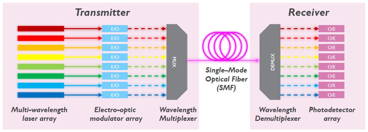
Schematic representation of a communication link employing DWDM with 8 wavelength channels
Such a WDM link requires the integration of various optical components. Si photonics is a preferred technology for integrating all the building blocks into a single chip. Integrated Si photonics exploits the CMOS infrastructure to manufacture optical circuits, realizing cost benefits through economies of scale. And it enables a high integration density, reduced power consumption and a high yield. Combined with the capabilities of WDM, highly scalable single-mode optical transceivers can be constructed. This technology offers a scaling path towards Tb/s optical ports: from 4x25Gb/s today (enabling 100Gb/s) to 8x50Gb/s (400Gb/s) and ultimately 16x100Gb/s ( 1.6Tb/s), where 4, 8 and 16 represent the number of wavelength channels deployed in the multi-wavelength laser array.
Imec’s Si photonics integration platform
The Si photonics platform developed by imec enables the implementation of a complete WDM architecture. The platform uses 200mm SOI wafers as a substrate. The fabrication process uses a modified 130nm CMOS flow augmented with 193nm lithography for all the waveguide patterning layers and Ge for the photodetectors. An additional oxide/poly-Si stack is deposited to allow for more degrees of freedom in the design of the optical components. This stack is used for integrating the advanced passive components, like grating couplers, waveguides and wavelength multiplexing filters. Within this integration platform, passive components as well as active components (such as opto-electronic modulators, heaters and Ge-on-Si photodetectors) can be co-integrated. Electronics circuits (like drivers and trans-impedance amplifiers or TIAs) can be fabricated on a separate die and assembled with the Si photonics circuits using flip-chip assembly methods. In these circuits, the driver converts a standard CMOS bit state into an electrical current that is compatible with the optical device, while the TIA amplifies the photocurrent into a standard CMOS bit state.
A 4x20Gb/s hybrid CMOS Si photonics transceiver
Significant research and development have resulted in the demonstration of the basic building blocks, such as high-speed photodetectors, modulators and (de-)mulitplexing filters. Recently, imec researchers have integrated all these building blocks in the same Si photonics platform to demonstrate a 4x20Gb/s hybrid CMOS Si photonics transceiver prototype (*ISSCC 2015).
Imec’s CMOS silicon photonics transceiver comprises a Si photonics chip, flip-chip integrated with a low-power co-designed 40nm foundry CMOS chip. The Si photonics chip, fabricated on imec’s 25Gb/s Si photonics platform, comprises an array of four compact 25Gb/s ring modulators, coupled to a common bus waveguide to allow WDM transmission. On the receive side, a ring-based, low-loss (2dB) de-multiplexing filter with 300GHz channel spacing is implemented and further connected to an array of four 25Gb/s Ge waveguide photodetectors. Both the ring modulators and the ring WDM filters include highly efficient integrated heating elements to tune their resonant wavelengths to the desired WDM channels. The CMOS chip includes four differential 20Gb/s ring modulator drivers and four 20Gb/s trans-impedance amplifiers. A 12 channel single-mode fiber array is packaged onto the grating coupler array on the chip, using a planar approach developed at Tyndall National Institute.
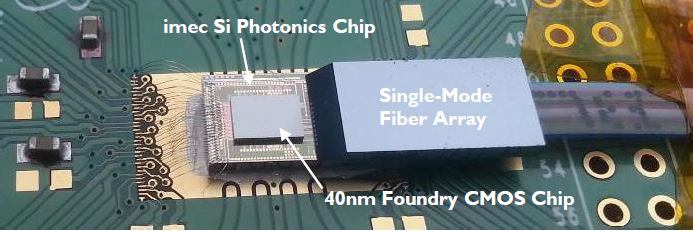
Hybrid CMOS Si photonics transceiver module
Error-free operation was demonstrated in a 20Gb/s loop-back experiment for all four WDM channels as well as with two channels running together. The four WDM wavelength channels consumed about 2mW per Gb/s (excluding laser and thermal control power). Thermal tuning of the WDM channel wavelengths consumed 7mW/nm per channel.
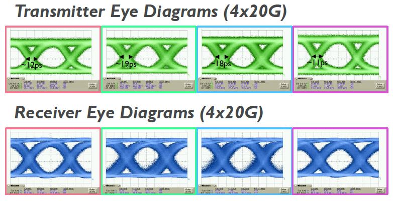
Measured 20Gb/s transmitter and receiver eye diagrams
Building blocks for a 8x50Gb/s DWDM Si photonics technology
The transceiver can be further scaled to higher bandwidth capacity by adopting more advanced CMOS technology and by adding more WDM channels. This will enable optical modules for 100Gb/s, 400Gb/s and beyond for future datacenter interconnects. Recently, imec has demonstrated several building blocks for 8x50Gb/s DWDM optical links, offering a clear scaling path towards 400Gb/s.
Among the main building blocks are optical modulators. To meet the 50Gb/s channel data rate, modulation efficiency and bandwidth have to be carefully balanced, and footprint and thermal robustness considerations have to be taken into account. Modulators can come in several flavors, such as Si ring modulators and Ge(Si)-based electro-absorption modulators, each having their own advantages and disadvantages. In general, ring-based modulators in silicon have a small footprint and low power consumption, but suffer from low optical bandwidth and require control circuits for compensating process and thermal variations. Alternatively, electro-absorption modulators offer a wider optical bandwidth than Si-based ring modulators. Imec has developed solutions for both types of modulators, each with modulation bandwidths beyond 50GHz.
The Ge waveguide electro-absorption modulator is implemented in imec’s Si photonics platform. This modulator, designed in a lateral p-i-n Ge/Si diode configuration, has a 3-dB bandwidth modulation greater than 50GHz and a junction capacitance as low as 12.8fF at -1V. While operating at a data rate of 56Gb/s, the device modulates light at 1610nm with a dynamic extinction ratio up to 3.3dB. Due to its ultralow capacitance, the total power consumption (dynamic and static) of the modulator is less than 2mW in typical operating conditions.
Imec also demonstrated a compact ring modulator enabling 56Gb/s modulation with a drive voltage as low as 2.5V peak-to-peak swing (Vpp). For the ring, the researchers used a partially etched waveguide with etched trench depth of 150nm and waveguide width of 500nm, enabling a ring radius of only 5 micrometer. Such a small ring size results in a large free spectral range, which can be exploited for multi-channel WDM applications. The small ring size also reduces the device capacitance. For 2.5Vpp and a device capacitance of ~30fF, the dynamic energy consumption of the device is approximately 45fJ/bit. 56Gb/s modulation is demonstrated with 4dB dynamic extinction ratio.
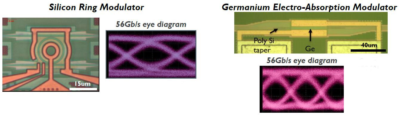
Si ring modulator and Ge electro-absorption modulator with measured eye diagrams
To complete the optical link, imec also developed a DWDM demultiplexing filter, and fiber and laser coupling structures. Both in-plane couplers (with less than 2dB loss over 100nm) and surface-normal couplers (with less than 3dB loss over 30nm) have been demonstrated. The platform further includes optical interfaces to hybridly integrate a III/V laser array on the Si photonics chips. For the detection of the WDM signals, imec developed a 50Gb/s Ge-on-Si waveguide photodetector. The detector has a vertical p-i-n diode configuration, with p-type contact in the Ge and n-type contact in the Si material.
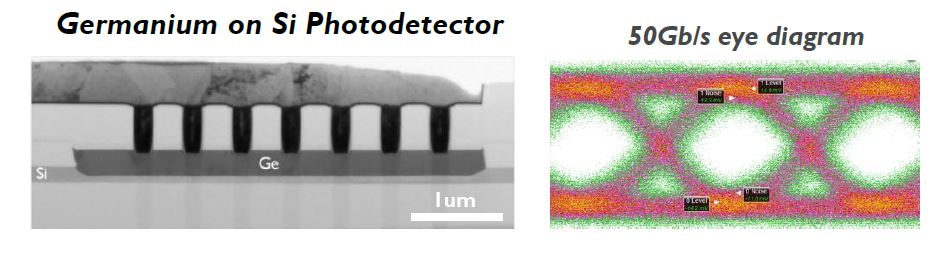
Ge-on-Si photodetector with measured eye diagram
Outlook and offering
Imec’s DWDM Si photonics technology offers a clear path to scale optical links towards 400Gb/s (8x50Gb/s). In the future, scaling to 1.6Tb/s (16x100Gb/s) becomes likely by adopting advanced modulation schemes such as pulse amplitude modulation (PAM)-4. Today, the platform allows co-integrating the various building blocks on 200mm wafers. Currently, imec researchers are developing a next-generation Si photonics platform on 300mm wafers, which will offer further improved optical performance and compatibility with the latest 3D integration technologies.
Companies can benefit from imec’s Si Photonics platform (iSiPP25G) through established standard cells, or by exploring the functionality of their own designs in multi-project wafer (MPW) runs. The iSiPP25G technology is available via imec IC-link services and MOSIS, a provider of low-cost prototyping and small volume production services for custom ICs.
More info
’Imec demonstrates compact wavelength-division multiplexing CMOS silicon photonics transceiver’, press release ISSCC 2015
‘Imec demonstrates 50GHz Ge waveguide electro-absorption modulator’, press release OFC 2015
‘The power of silicon photonics for telecom and datacom’, imec magazine, September 2014