Build your GaN-ICs with imec’s GaN-on-SOI MPW process
The advantages of GaN (gallium nitride) as a power conductor are increasingly obvious. So is the need to integrate GaN power devices on a single chip. Imec tackles that challenge with its unique GaN-on-SOI process. And it’s affordable to you thanks to imec’s Multi-Project Wafer service (MPW).
GaN-ICs unlock the full potential of GaN power electronics
Most current GaN-based power systems are multi-chip solutions: different components are assembled on a PCB. Not ideal, because maximum switching speeds don’t even come close to their potential values.
The better solution is to combine these components on one complex GaN-IC. That allows you to:
- minimize form factors
- increase switching speeds
- save on packaging costs
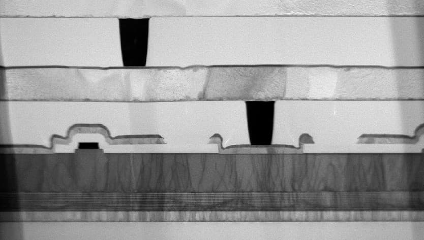
So how do you tackle that monolithic integration? The biggest challenge is the lateral isolation of the devices to minimize parasitic inductance. In GaN-on-Si devices, that’s achieved by an isolation implant or a mesa etching process. Not ideal, because the devices still share a common conductive Si substrate, which can only be referenced to a single potential at a time.
Imec researchers have worked out a better way: grow GaN on SOI wafers and use trench isolation. This technique has been extensively tested, with excellent results.
In 2022, d-mode HEMTs and Schottky barrier diodes were also added to imec's GaN IC portfolio. Check out the research update
MPW makes GaN-IC’s affordable
Are you looking to produce Gan-IC’s in small quantities or prototypes? You have easy and affordable access to imec’s expertise and its state-of-the-art facilities. Take advantage of our Multi-Project Wafer service (MPW) in order to share mask, processing and engineering costs with multiple partners. And design your own GaN-IC’s using our Process Design Kit (PDK).
If you’re ready to produce medium to high volumes of GaN-IC’s, feel free to contact us for dedicated mask runs.