Partner related news
Europe’s bid for leadership in photonic chips begins in Barcelona
About PIXEurope
PIXEurope is the fifth Pilot Line initiative launched through the European Chips Joint Undertaking, established under the European Chips Act, to accelerate the development of photonic integrated circuit (PIC) technology, a critical enabler for high-speed computing, communications, quantum information systems, and beyond. The Pilot Line is a shared European industrial platform where companies (from startups to large corporations) can design, prototype, test, and validate photonic chips more quickly and at lower risk before large-scale manufacturing. It will be Europe's first fully integrated, distributed Pilot Line connecting the entire PIC value chain, from design and fabrication to integration, packaging, and testing, across multiple coordinated European sites within a unified and standardized framework.
With a budget of €400 million and the participation of 20 institutions from 11 European countries (Austria, Belgium, Finland, France, Ireland, Italy, Poland, Portugal, Spain, the Netherlands and the United Kingdom), PIXEurope will master key technology platforms spanning a broad range of materials - from silicon and silicon nitride to indium phosphide, lithium niobate, and beyond - and the integration of photonic and electronic chips.
Now in its second year of operation, PIXEurope has moved from setup into early delivery. More than 100 companies and research and technology organizations have already engaged with the Pilot Line through technical discussions and exploratory collaborations, spanning the full PIC value chain. As of May 2026, four of the five planned service lines are already operational: consultancy, training, prototyping, and participation in collaborative R&D projects. From November 2026, users will be able to access existing partner infrastructures, with new Pilot Line infrastructures becoming available from May 2027. Full operational capacity - including Multi-Project Wafer runs and all five service lines - is expected by May 2028.
The Pilot Line will serve companies of all sizes through a centralized open-access gateway, with the ultimate goal of creating a unique and thriving European PIC ecosystem - reducing time-to-market, lowering risks and costs, and transferring technologies with demonstrated maturity to large-volume manufacturers for scalable industrial production. In doing so, PIXEurope represents a decisive step toward European technological sovereignty in photonics, bridging the gap between scientific research and industry for the decades ahead
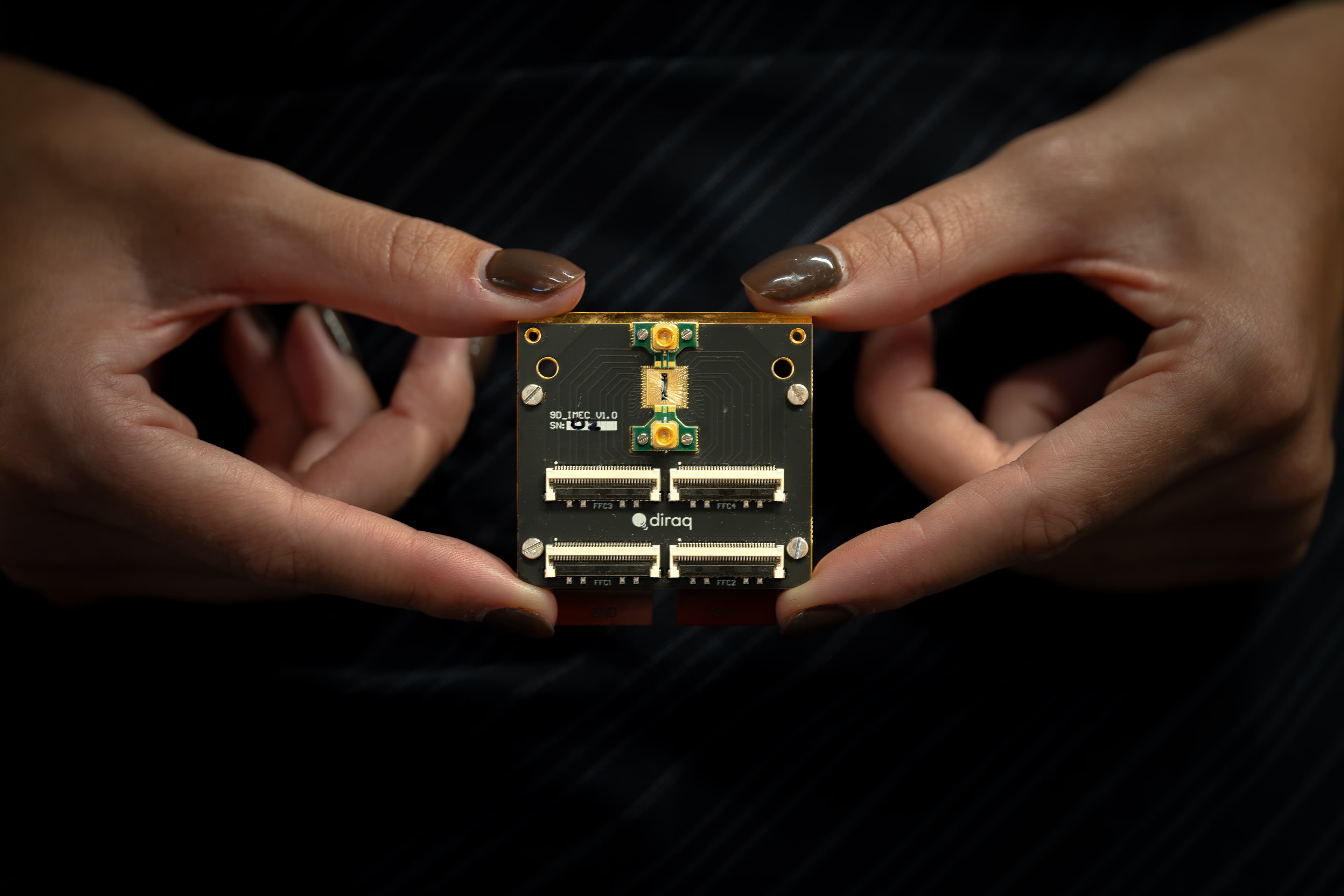
Role of imec
Imec plays a central role in delivering key technologies and capabilities for the advanced photonic integrated circuits pilot line. imec contributes major silicon‑based photonics platforms, hybrid integration technologies, advanced packaging solutions, and demonstrator developments that are essential for establishing a scalable, industrially relevant, and open‑access European pilot line.
Within the project, imec is a primary contributor to the development and advancement of silicon photonics platforms, notably through its thin silicon‑on‑insulator technologies, including the mature iSiPP and iSiPP300 platforms. These platforms support fabrication on 200 mm and 300 mm wafers and provide a comprehensive set of active and passive photonic building blocks. They form a foundational capability for applications in datacom, telecom, sensing, LiDAR, and computing, and enable the transition from research‑grade photonic integration toward high‑volume, industrial manufacturing.
imec also plays a key role in hybrid and heterogeneous integration activities, particularly through the development and application of micro‑transfer printing and fine‑pitch interconnection technologies. The institute contributes processes for integrating III‑V materials, thin‑film lithium niobate, and other advanced functional materials onto silicon photonics platforms, while developing advanced back‑end‑of‑line processes such as copper micro‑bump integration to enable tight electronic–photonic co‑integration. These activities are critical for improving yield, scalability, and manufacturability of complex photonic‑electronic systems.
In the area of packaging, imec contributes wafer‑level and chiplet‑based packaging technologies that support high‑density electrical and optical interconnects. Its work on fine‑pitch micro‑bump processes and co‑packaged optics enables the convergence of photonics and electronics in architectures compatible with advanced CMOS manufacturing, directly addressing scalability requirements for emerging mass‑market applications.
imec is furthermore strongly involved in technology validation through the development of PIXEurope demonstrators, including demonstrators targeting co‑packaged optics and electronics for artificial intelligence and data‑center applications. These demonstrators validate the integration of imec’s silicon photonics platforms with hybrid integration and advanced packaging technologies and serve to demonstrate interoperability across the distributed pilot line.
Through its role as a major pilot‑line service provider, imec supports PIXEurope’s open‑access strategy by offering advanced fabrication, integration, and packaging capabilities that are fully aligned with the project’s design kit methodology, including process, assembly, and test design kits. In doing so, imec ensures strong industrial relevance, supports technology transfer, and enables European companies, SMEs, and research organizations to scale photonic innovations from prototype to manufacturing