/EUV imaging at Hyper NA

EUV imaging at Hyper NA

PhD - Brussel | More than two weeks ago

Can we continue semiconductor scaling by increasing the NA for EUV lithography?

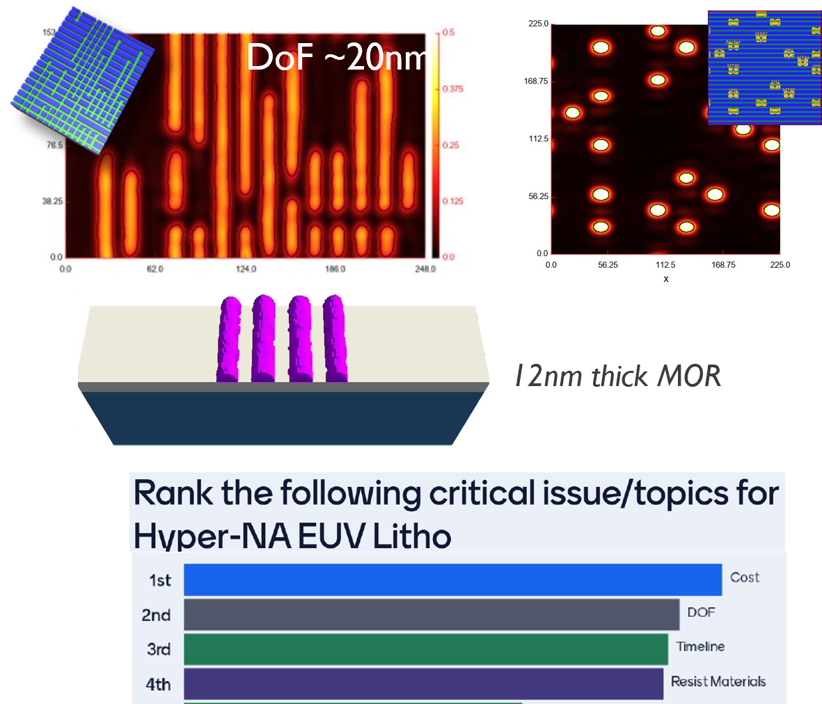
To continue scaling semiconductor devices, we need to be able to print ever smaller structures. Currently, this can be achieved with high NA EUV lithography. In the future, the next logical step is to increase the NA further to so called hyper NA systems. This comes with some challenges however: depth of focus will shrink which will require thinner photoresist. Also, intrinsic resist granularity will become more important at smaller dimensions. The first goal of the thesis is therefore to model photoresist to find what is needed for hyper NA. The second part is to understand the usefulness of hyper NA. This requires identifying patterning cliffs for various designs that could be enabled by a higher NA as well as mask/imaging solutions to push this limit further. 

As part of the “Imaging and Reticles” team within the Advanced Pattering department of imec in Leuven, you will work alongside a group of dedicated researchers, who study the optical image formation process in the most advanced lithography system in the world and its dependency on all aspects of the photomask. In addition, you will be enrolled in the Katholieke Universiteit Leuven during your PhD studies.


Required background: Physics, material science, material modeling

Type of work: 70% modeling, 20% experimental, 10% literature

Supervisor: Stefan De Gendt

Co-supervisor: Vicky Philipsen

Daily advisor: Joern-Holger Franke

The reference code for this position is 2026-004. Mention this reference code on your application form.

Who we are
Accept analytics-cookies to view this content.
imec's cleanroom
Accept analytics-cookies to view this content.

Related jobs

Computer Vision for Defect Inspection and Metrology: Solving Semiconductor Manufacturing Challenges towards Advanced Process Control using Machine Learning

This internship project addresses fundamental computer vision challenges arising from this domain, with the semiconductor process flow providing the boundary conditions and practical constraints. 

Area-selective deposition of single-biomolecules using DNA/protein origamis

Explore area-selective deposition at the interface of chips and biomolecules to revolutionize the future of biosensing and biosynthesis.

Exploration of the mechanisms of Atomic Layer Etching to enable anisotropic etching of Co-based alloys

Become a metal nano-carver to build next-generation CMOS!

[NanoIC topic] Research on High Aspect Ratio Dielectric Etch for 3D Integration

Understand mechanisms governing the cryogenic plasma etch processes and fabricate high aspect ratio patterns for the memory and logic technology nodes of the future.

[NanoIC topic] Illuminating the Future of Nano-Etching: Join imec’s Angstrom Patterning Department PhD Program

Pioneer ultraviolet light-driven etching techniques for next-generation semiconductor and photonic devices.

[NanoIC topic] Mathematical Statistical methods for ML algorithms for EUVL

Build up Mathematical Statistical innovative methods to create Machine Learning algorithms and models, tuned to accurately predict and automate characterization of defect-limiting, stochastic-induced, effects on device performance (yield), explicit to massive EUV-patterning proce
Job opportunities

Send this job to your email