Towards a high-throughput AI-driven multi-modal and multi-tip electrical AFM platform for nanoelectronics device analysis
PhD - Leuven | More than two weeks ago
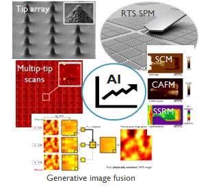
Atomic force microscopy (AFM) has become a powerful tool for nanoelectronics device analysis and a variety of electrical modes has become available to investigate diverse nanoscale electronic properties which opens new opportunities for correlative research. The general practice is hereby to sequentially acquire several types of signals from the same region of interest of the sample, for example, spreading resistance maps in scanning spreading resistance microscopy (SSRM), differential capacitance maps in scanning capacitance microscopy (SCM) or current maps with conductive atomic force microscopy (C-AFM). Each dataset is then processed independently and compared visually, from which conclusions are drawn about the correlation between sample’s structural and electrical features. However, the different AFM modes require distinct hardware components and switching between them takes a lot of time and can disrupt the workflow. Furthermore, electrical AFM measurements do not directly probe the intrinsic properties of the material but instead, they reflect the complex interactions between the AFM tip and the sample. Every AFM map including those capturing electrical signals is influenced by the geometry and condition of the tip, making it difficult to distinguish genuine sample characteristics from tip-induced artifacts. Moreover, the physics underlying the tip–sample interactions in electrical AFM modes remains only partially understood and is highly complex, governed by non-linear, mode-specific, and tip-dependent factors. In theory, one way to deconvolve these tip-related effects would be to perform repeated measurements using different tips across various modes and perform deep analysis of the results. In practice, however, this approach is nearly unfeasible. Switching modes and replacing tips in standard electrical AFM introduce cumulative time delays between the measurements, both labor-intensive and costly, and are thus highly impractical. Additionally, there is inherent variability among AFM probes, even within the same production batch. As a result, cantilever spring constants may differ slightly between tips, leading to variations in force control and affecting the accuracy of tip-sample interaction measurements.
Therefore, in this PhD project these challenges are addressed by exploiting the unique features of the recently established reverse tip sample (RTS) scanning probe microscopy (SPM), where the sample is mounted on the cantilever, allowing for fast and easy tip switching along with consistent force application between the tips. Custom hardware will be designed and prototyped and elaborated automation routines will be established to efficiently collect large datasets across various electrical modes and tips. To enable and facilitate the mixing and correlation of the collected signals, advanced computational techniques such as AI-driven data fusion and cross-correlation on a pixel-by-pixel basis are going to be explored for extracting deeper insights from multimodal datasets. Furthermore, the precise control of instrument noise is studied for achieving true signal mixing, and the interpretation of multidimensional statistical data is explored. The final targeted outcome of this PhD research is the establishment of powerful AFM platforms that offer seamless, real-time multi-modal electrical signal acquisition, enhanced by intelligent algorithms that both optimize data collection and analyze the results. These algorithms could help to remove tip-related artifacts from the signal, revealing previously hidden correlations or emergent behaviors. The ability to obtain a comprehensive electrical perspective, unconstrained by tip shape or size, will be a crucial enabler to adequately characterize next-generation nanoelectronics devices which continue to shrink and grow more complex.
Required background: Electrical engineering, solid-state physics, material science, semiconductor manufacturing
Type of work: 50% experimental, 40% analysis & programing, 10% literature
Supervisor: Anne Verhulst
Daily advisor: Nemanja Peric
The reference code for this position is 2026-065. Mention this reference code on your application form.