Press release
Imec Achieves Record-Low Source/Drain Contact Resistivity for PMOS Transistors
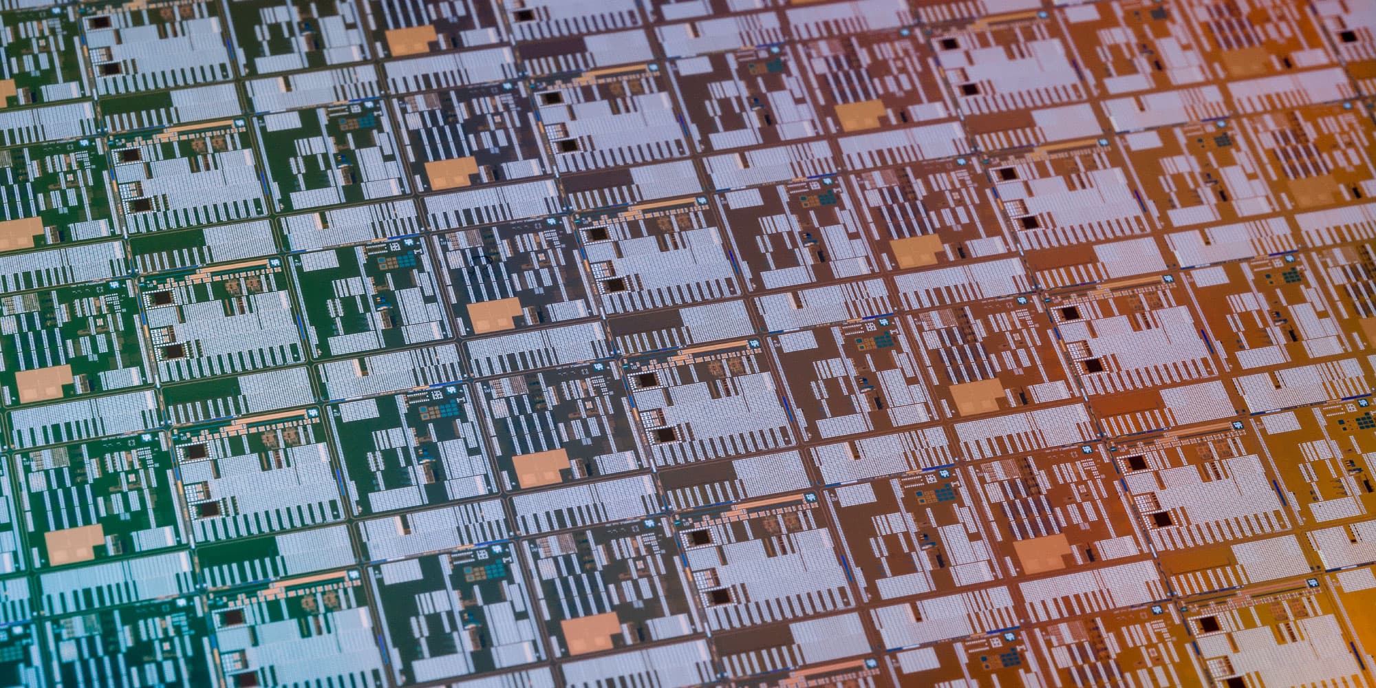
KYOTO (Japan) – June 08, 2017 – At this week’s 2017 Symposia on VLSI Technology and Circuits, imec, the world-leading research and innovation hub in nano-electronics and digital technology, reported record breaking values below 10^-9 Ohm.cm² for PMOS source/drain contact resistivity. These results were obtained through shallow Gallium implantation on p-SiliconGermanium (p-SiGe) source/drain contacts with subsequent pulsed nanosecond laser anneal.
In future N7/N5 nodes, the source/drain contact area of the transistors becomes so small that the contact resistance threatens to become the dominating parasitic factor, resulting in suboptimal transistor functioning. Researchers have therefore been working on techniques to reduce the contact resistance on highly doped n-Si and p-SiGe source/drain contacts, aiming for values below 10^-9 Ohm.cm². Together with colleagues from the KU Leuven (Belgium), Fudan University (Shanghai, China), and Applied Materials (Sunnyvale, USA), imec’s specialists concentrated on p-SiGe contacts, comparing the effects of high-dose Boron and Gallium doping.
For the comparison, the researchers implanted SiGe separate wafers with a high dose of Gallium or Boron and applied various anneal processes. They then fabricated multi-ring circular transmission line model structures, which are highly sensitive to contact resistance. Subsequent measurements revealed the lowest contact resistance for the Gallium-implanted structures annealed with Applied Material’s nanosecond laser anneal. This process uniquely causes a Ge/Ga surface segregation, which is responsible for the ultralow sub-10^-9 Ohm.cm² contact resistivity. This result show a possible way to process next-generation technology nodes.
Naoto Horiguchi, distinguished member of the technical staff at imec indicated: “This breakthrough achievement in our search to develop solutions for next generation deeply-scaled CMOS provides a possible path for further performance improvement using the current source/drain schemes in N7/N5 nodes.”
Imec’s research into advanced logic scaling is performed in cooperation with imec’s key partners in its core CMOS programs including GlobalFoundries, Huawei, Intel, Micron, Qualcomm, Samsung, SK Hynix, Sony Semiconductor Solutions and TSMC.

About imec
Imec is the world-leading research and innovation hub in nano-electronics and digital technologies. The combination of our widely acclaimed leadership in microchip technology and profound software and ICT expertise is what makes us unique. By leveraging our world-class infrastructure and local and global ecosystem of partners across a multitude of industries, we create groundbreaking innovation in application domains such as healthcare, smart cities and mobility, logistics and manufacturing, and energy.
As a trusted partner for companies, start-ups and universities we bring together close to 3,500 brilliant minds from over 75 nationalities. Imec is headquartered in Leuven, Belgium and also has distributed R&D groups at a number of Flemish universities, in the Netherlands, Taiwan, USA, China, and offices in India and Japan. In 2016, imec's revenue (P&L) totaled 496 million euro. Further information on imec can be found at www.imec-int.com.
Imec is a registered trademark for the activities of IMEC International (a legal entity set up under Belgian law as a "stichting van openbaar nut”), imec Belgium (IMEC vzw supported by the Flemish Government), imec the Netherlands (Stichting IMEC Nederland, part of Holst Centre which is supported by the Dutch Government), imec Taiwan (IMEC Taiwan Co.) and imec China (IMEC Microelectronics (Shanghai) Co. Ltd.) and imec India (Imec India Private Limited), imec Florida (IMEC USA nanoelectronics design center).
Contact
Hanne Degans, Press communication manager, T: +32 16 28 17 69, Mobile : +32 486 06 51 75, Hanne.Degans@imec.be


