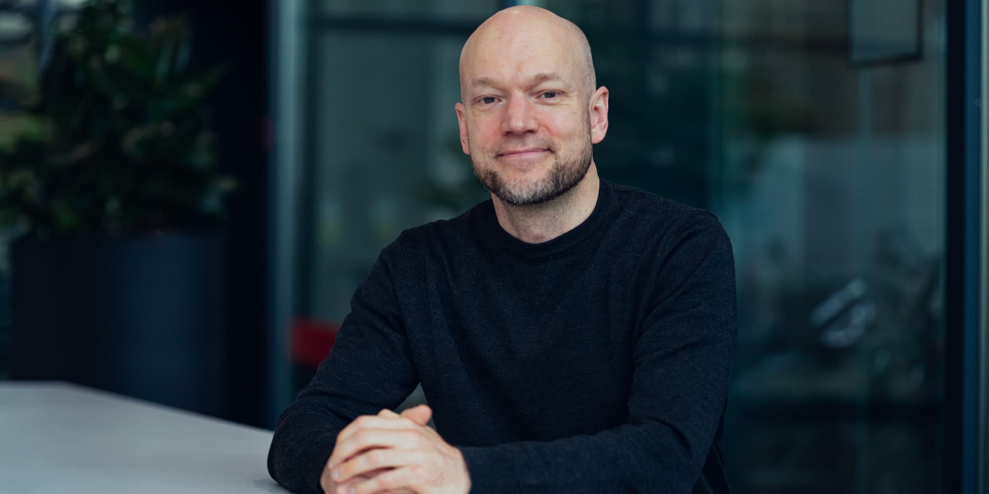

For more than four decades, Dr. Mircea Dusa has worked at the center of semiconductor lithography, the field that makes it possible to print ever-smaller, more precise patterns on chips.
As an imec fellow currently working on sub-10-nm patterning, Mircea brings together a rare breadth of knowledge across exposure tools, mask making, metrology, process control, and the co-optimization of chip design with patterning processes. His career spans the evolution of lithography from earlier optical systems to today’s most advanced immersion and EUV technologies.
A career shaped by lithography scaling
Mircea received a master’s degree in electrical engineering and solid-state physics, followed by a doctorate in applied optics from the Polytechnic University of Bucharest. That combination of electrical engineering, physics, and optics became the foundation for a career focused on one of the semiconductor industry’s most demanding challenges: printing smaller features with ever-higher accuracy and reliability.
Before officially joining imec in 2019, Mircea spent 20 years at ASML, the world-leading supplier of lithography equipment. For a decade as ASML Fellow resident at imec, he already made a significant impact in strengthening the alignment between imec’s patterning strategies and ASML’s advanced lithography roadmap, with a particular focus on the patterning ecosystem and the advancement of EUV lithography.
One notable achievement was the creation of the Advanced Patterning Center (APC), a structure that attracted key patterning suppliers and became the test floor for ASML as well as many other suppliers’ product introductions. Included in APC strategy was imec’s installation of all ASML new generation holistic lithography products, with a remarkable example for the High NA EUV lithography scanner, the most complex semiconductor production tool enabling sub-10nm scaling for AI devices.
His work as an ASML Fellow resident at imec translated into more than 40 joint papers, published in global peer-review journals and presented at the world’s most respected technical conferences.
Earlier in his career, he held engineering and R&D roles at Fairchild Research Center of National Semiconductor, Zygo Corporation, SEEQ Technology, Technical Instruments, and ICCE Bucuresti. Across these roles, he worked in both research and manufacturing environments, gaining a practical understanding of what it takes to move advanced lithography concepts into real production.
Enabling the next generations of patterning
Throughout his career, Mircea contributed to technologies that enabled continued semiconductor scaling from one technology node to the next. He pioneered work in multi-patterning, a set of techniques that allow chipmakers to create features smaller than what a single lithography exposure can reliably print. He also contributed to the development and manufacturing introduction of spectroscopic diffraction-based scatterometry metrology, a key method for measuring and controlling patterned structures on wafers.
In addition, Mircea authored papers on lithography process control using diffraction-based metrology for critical dimension (CD) and overlay. The paper “Normal incidence spectroscopic ellipsometry and polarized reflectometry for measurement and control of photoresist critical dimension”, was an industry first on the industrial application of diffracted-based optical metrology enumerated in the Smithsonian/NASA Astrophysics Data System digital library.
These contributions reflect a broader strength in Mircea’s work: connecting deep physical understanding with manufacturable solutions. Lithography is not only about printing patterns; it is about managing an entire system of interacting variables. Pattern fidelity, overlay, imaging, process windows, masks, materials, and design constraints all need to be understood together.
That system-level view has become increasingly important as the industry moves into sub-10nm dimensions. At these scales, small variations can have major consequences. Progress depends on the ability to combine advanced tools, precise metrology, robust process control, and design-aware patterning strategies.
Bringing holistic lithography expertise to imec
Mircea joined imec in 2019, where he continues to work on advanced patterning for future semiconductor technologies. As an imec fellow, he contributes not only technical expertise, but also decades of accumulated insight into how lithography innovations mature from scientific concepts into industry-ready capabilities.
His background makes him especially valuable in a research environment where collaboration across disciplines is essential. Advanced patterning sits at the intersection of physics, optics, materials, equipment engineering, process integration, design, and manufacturing. Mircea’s career has touched each of these areas, allowing him to help teams connect detailed technical decisions to the bigger scaling roadmap.
Mircea has authored more than 250 technical publications and holds around two dozen US patents in lithography and metrology.

Dr. Mircea V. Dusa is an imec fellow working in the field of sub-10nm patterning. He has more than 40 years of experience in the semiconductor industry, with expertise spanning exposure tools, mask making, metrology, process control, and the co-optimization of design and patterning processes.
Before joining imec in 2019, Mircea spent 20 years at ASML, where he was an ASML Fellow working on exploratory activities to enhance immersion and EUV exposure tools as holistic systems. He holds a master’s degree in electrical engineering and solid-state physics, and a PhD in applied optics from the Polytechnic University of Bucharest.
Expertise
- Sub-10-nm patterning
- Lithography and optical systems
- Metrology and process control
- Design-patterning co-optimization
Career highlights
- Joined imec in 2019 as an imec fellow working on advanced sub-10-nm patterning
- Was an ASML Fellow resident at imec for 10 years, working on immersion and EUV lithography systems
- Worked 20 years for ASML as a senior imaging scientist, where he was a founding member of the Technology Development Center and was recognized as one of the company’s first ASML Fellows
- Pioneered enabling technologies for semiconductor scaling, including multi-patterning and spectroscopic scatterometry metrology
- Authored more than 250 technical publications and holds around two dozen US patents in lithography and metrology
- Is a SPIE Fellow and has chaired major SPIE lithography conferences where he taught one of the most successful SPIE courses covering the principles of multi-patterning
Published on:
4 August 2026