Customized laser design for integration with silicon photonics
Develop your photonic chip with a tailored integrated light source on imec’s proven platforms and guide it all the way to prototyping and manufacturing.
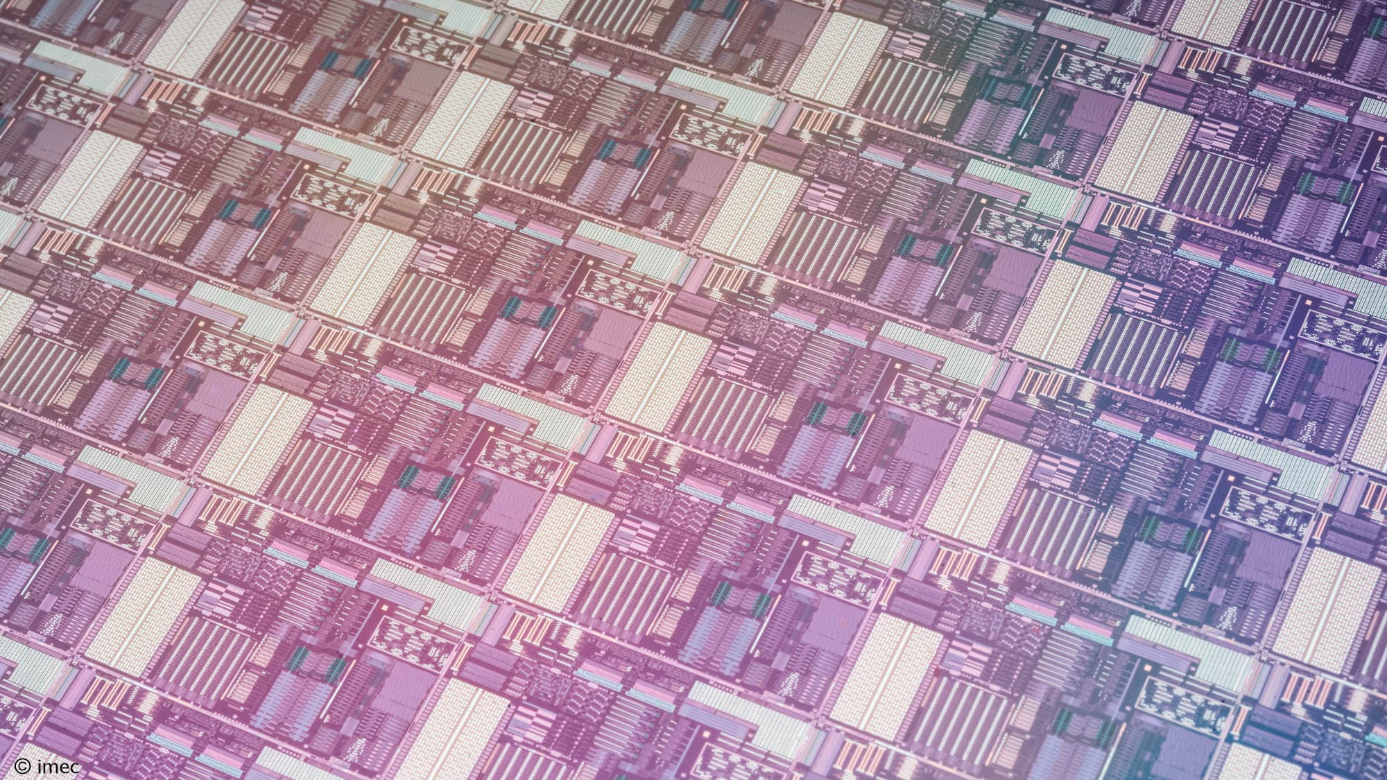
Advanced photonic integrated circuits (PICs) are able to boost the performance of a wide range of applications such as optical communications, optical 3D sensing, metrology, gas sensing, and lidar. A crucial factor in the effectiveness of these PICs is their light source:
- It needs to be tailored to the needs of the application.
- It’s best integrated on the chip to enable low-cost, high-yield and high-volume manufacturing.
- To optimize performance, it’s ideally co-designed with the electronics and the hybrid integration methods – such as flip-chip bonding.
This is why imec has extended the capabilities of its silicon photonics platform (iSiPP) with customized light sources that can be integrated on the PIC to enable low-cost, high-yield and high-volume manufacturing.
This project received funding from the PhotonDelta National Growth Fund program.
Integration of InP lasers and SiN waveguides
To achieve the highest possible performance for your PICs, imec offers customized laser design services. We can provide indium phosphide (InP) laser dies and gain chips. Imec’s silicon nitride (SiN) platform allows for efficient coupling and spectral control of entire gain sector arrays, via customized external cavity design.
Recently, imec has proved hybrid integration through passive alignment of InP to SiN. To enable applications such as (bio)sensors, communications and lidar, the targeted specifications are:
- > 100 mW optical output power
- < 10 kHz Lorentzian linewidth
- > 100 nm tuning range (around C-band)
The combination of InP and SiN technologies allows you to add multiple infrared light sources to your PIC design. Reference designs are available in the O- and C-band. Upon request, additional wavelengths can be considered, addressing the fields of optical communication, sensors, computing, and lidar.
Hybrid laser integration for high-volume throughput
A flip-chip route to high-volume manufacturing is available, built on 200- and 300mm silicon photonic wafers, including a wide range of active and passive devices.
The interface for flip-chip distributed feedback (DFB) laser integration has been developed in imec’s iSiPP200N platform. In addition to high-speed electro-optic Si modulators, high-bandwidth germanium (Ge) photodetectors and efficient thermo-optic heaters, this platform includes highly uniform low-pressure chemical vapor deposition (LPCVD) SiN waveguides, with low loss and accurate phase control, enabling the synthesis of high-quality, precise filters and complex circuits.
Work with us
Are you looking for a partner to develop your advanced PIC – including an integrated light source? Imec is ready to:
- Provide the necessary technologies based in its tested and proven silicon and silicon nitride platforms.
- Design, develop, and prototype your photonic chips, leveraging its vast expertise and unique infrastructure.
- Manufacture your product in low volumes and seamlessly guide you to high-volume production in one of our partner foundries.