Silicon nitride-based photonics
Take advantage of imec's 200-mm commercial platforms for the dedicated development of your SiN-based photonic ICs.
Very low propagation loss, high power handling, CMOS compatibility, ... There are many reasons why silicon nitride (SiN) is the ideal platform for photonic integrated circuit (PIC) applications such as LiDAR, gas sensing, bio-spectroscopy, communication. And for uses in the quantum domain, such as quantum key distribution (QKD), quantum computing and quantum sensing.
Explore the many silicon nitride applications
Yet the development of SiN photonic ICs is still far from a routine workflow. Especially if the vision is to reach manufacturing as fast as possible, you might find it difficult to overcome the practical and financial hurdles on the road to dedicated photonic chip design, prototyping and manufacturing.
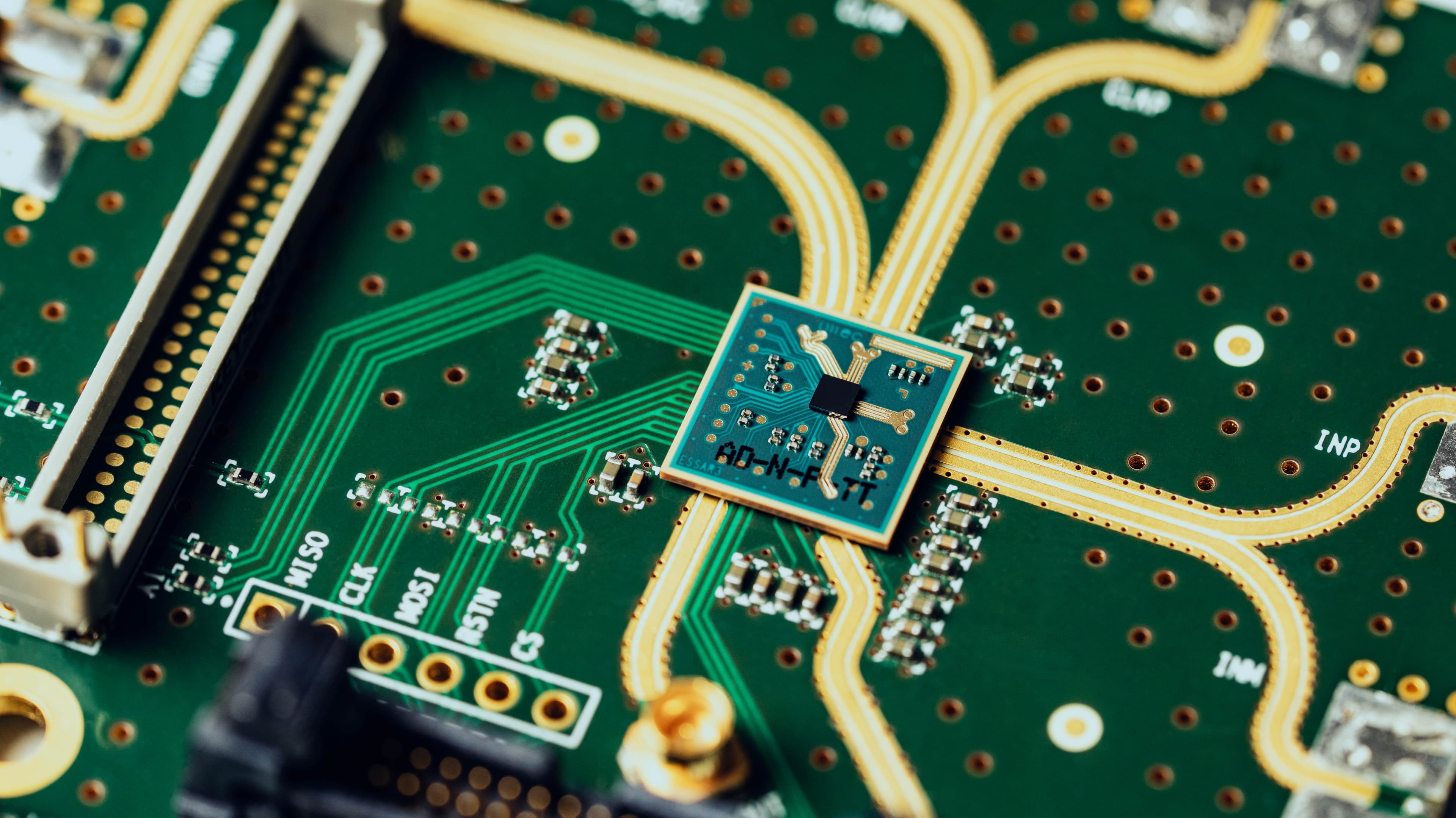
As an R&D hub, imec is one of the pioneers in silicon nitride integrated photonics. We offer access to nitride-based photonics in different ways: LPCVD low-loss SiN, CMOS-compatible PECVD SiN and co-Integrated Si/SiN.
Whether for research or product development, such technologies are accessible from early prototyping up to volume manufacturing.
Advantages of silicon nitride photonics
For integrated photonic applications that use visible and near-infrared light, silicon nitride is the perfect material. It combines:
- transparency for visible and near-infrared wavelengths – ideal for waveguides with low propagation loss (<0.1 dB/cm down to 2 dB/m)
- compatibility with CMOS technology – and therefore wafer-scale manufacturability at all volumes
- watt-range power handling thanks to low two-photon absorption
- low temperature sensitivity – providing stable performance for applications with wide temperature variation
- integration capability of active components – gain material (InP SOA, lasers) as well as high-speed modulators and Ge detectors
- custom-manufacturing flexibility – providing freedom for deposition of different layers with variable thickness: SiN layer on SOI, grating coupler optimization, Bragg reflector implementation, ...

SiN wafer
Key technologies
Depending on your application, imec offers you access to various silicon nitride photonic technologies:
1. High-temperature SiN
This platform, based on low pressure chemical vapor deposition (LPCVD), is the most suited SiN deposition method for integrated photonic applications requiring ultra-low loss such as photonic quantum applications, data/telecommunication and generally large PICs requiring low insertion loss.
The LPCVD technology combines:
- extremely low waveguide loss: <0.1 dB/cm down to 2 dB/m
- tight process control on full 200-mm wafers
- wide wavelength range: from 405 nm up to 2500 nm
- full library of passive components: grating couplers, splitters, ring resonators, directional couplers, ...

Grating coupler sample (LPCVD)
2. Low-temperature SiN
This SiN platform based on plasma-enhanced chemical vapor deposition (PECVD) is especially suited for applications such as integrated photonics on CMOS imagers and flat optics.
The PECVD technology combines:
- wide wavelength range: from 405 nm up to 2500 nm
- low waveguide loss: <2 dB/cm
- undetectable auto-fluorescence, ideal for spectrometers
- possibility to post-process silicon nitride photonics on CMOS, such as imagers
Both LPCVD and PECVD can be used for integrated photonic applications such as LiDAR/optical beamforming and standalone sensors (spectrometers) for life sciences.
3. Co-Integration of SiN photonics in complex build-up
This custom technology enables designers to benefit from the combination of SiN with other existing technologies such as CMOS and nonstandard SOI photonics.
Silicon nitride technology is compatible with:
- integration of layers into established SOI technologies and layer stack optimization towards your application
- custom integration on CMOS
- passive stack with multilevel LPCVD layers
- low-loss interface access for InP dies (laser, SOA) integration
Development of your silicon nitride-based photonics components
Imec assists you with the dedicated development process of your silicon photonics component. Based on your requests, we:
- assess the feasibility and map your device on our different technologies
- design the component and develop the process
- realize a first prototype
- optimize the design and process technology
- provide pilot line chip manufacturing
- transfer your process for high-volume manufacturing
Without delays or risks, you’re ready to hit the market with an innovative, reliable photonic core for your future product.
Work with us
Are you looking to accelerate your development?
Imec not only helps you to address technological challenges. Thanks to our thorough knowledge of the integrated photonics ecosystem, we can function as your full-fledged strategic partner – right down to venturing support.
Click the button below to get in touch.