Exploration of the mechanisms of Atomic Layer Etching to enable anisotropic etching of Co-based alloys
PhD - Leuven | More than two weeks ago
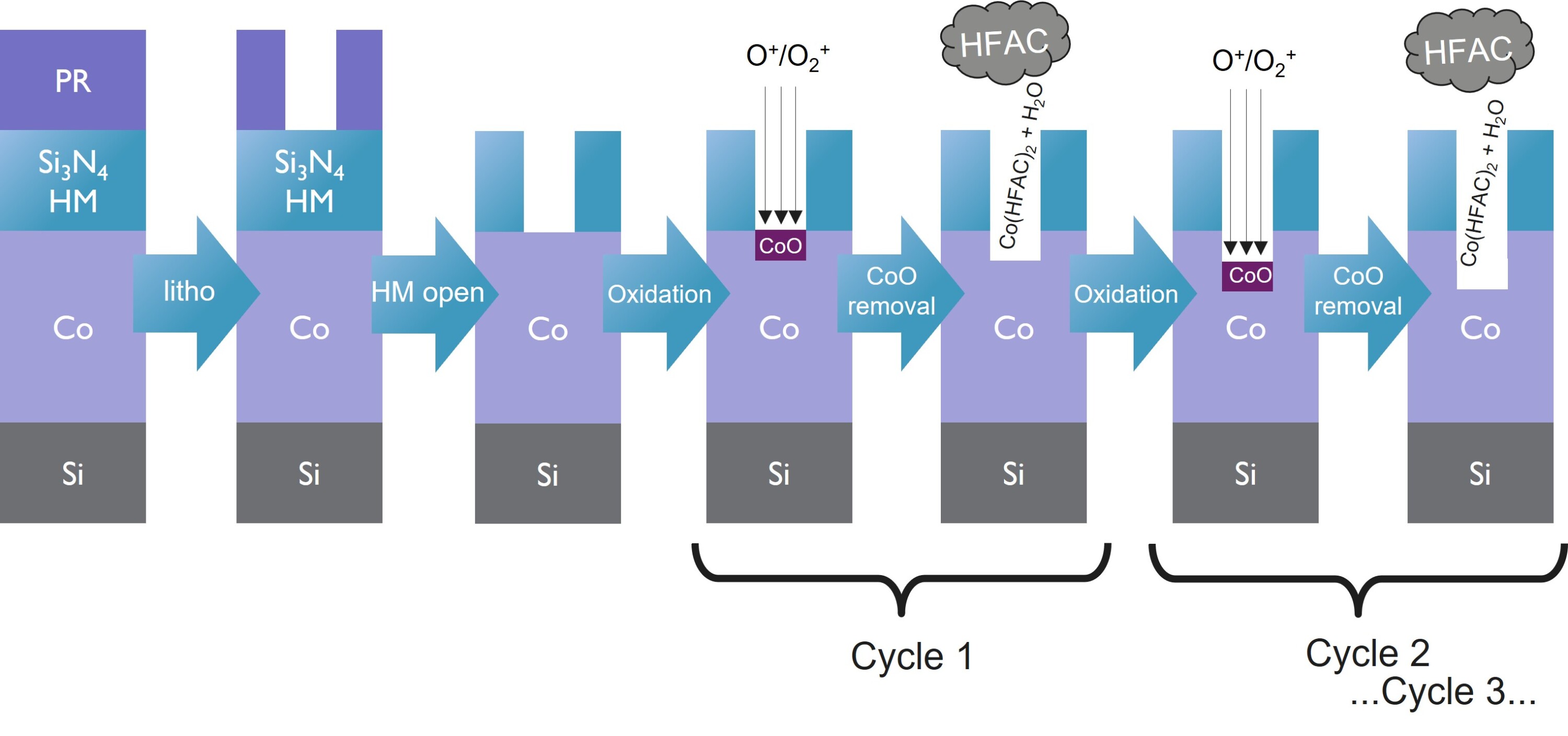
Advanced nano-electronic device manufacturing requires the introduction of new materials to fulfil new device requirements and functionalities: lower resistivity of nano-interconnect structures, larger photon absorbance for EUL masks, advanced magnetic layers for spintronics and memory, etc... A new paradigm in material design is achieved by moving from single elements to binary or ternary alloys, generally containing one transition metal (e.g. Ti, V, Mn, Fe, Co, Ni, Cu, Zn). The most straightforward integration of new alloys requires the (local/partial) removal of these layers to form an alloy nanopattern. The removal specifications depend on the application: isotropic/anisotropic; selective/non-selective; thick layers or residues. Additional constraints can appear, such as the temperature processing window, level of sidewall damage, etc.
Plasma based etching is challenging for most transition metals due to the low volatility of the (mostly halogen-based) reaction products. Interestingly, recent studies demonstrate that plasma activation combined with a vapor etch can act synergistically to enable the removal of complex alloys even at low temperatures (from room temperature to 350°C). This combined approach, typically applied in the forms of multiple cycles, is commonly referred as Atomic Layer Etching (ALE). The wide range of activation mechanisms (chemistry, plasma, ion beam, etc…), and large number of molecules for chemical reactions in the vapor phases (organic acids) open exciting avenues for the exploration of novel etch and clean mechanisms by ALE.
The main objective of this PhD research is to generate fundamental understanding into the mechanisms and design space of ALE of Co-based alloys. Cobalt-based alloys are central in this research in view of the high interest in cobalt alloys for memory, spintronics, EUVL mask absorbers and nano-IC applications (CoFeB, CoTa, CoSn or CoPtO2). We will explore the fundamental mechanisms during ALE of uniform thin films as well as nanopatterned arrays (for pattern transfer exploration). Insight into the chemical and physical changes during etching will be obtained based on the combination of complementary material characterization techniques including spectroscopic ellipsometry, X-ray reflectivity, transmission electron microscopy, Rutherford backscattering spectrometry, X-ray photo-electron spectroscopy, X-ray diffraction, atom probe tomography. To be compatible with device manufacturing technical constraints for commercial equipment, the quest for novel methods will focus on low temperatures (20-200°C), low pressure (mT to Torr) and in-situ processes (all sub-cycles performed in a single reactor).
Required background: Master in chemistry, physics, engineering or nanosciences
Type of work: 60% experimental, 30% analysis, 10% literature
Supervisor: Annelies Delabie
Co-supervisor: Jean-Francois de Marneffe
Daily advisor: Jean-Francois de Marneffe, Dennis van Dorp
The reference code for this position is 2026-178. Mention this reference code on your application form.