PhD Position: Exploring Thermal Imaging Techniques for Fault Detection in Future Semiconductor Nodes
PhD - Leuven | More than two weeks ago
As semiconductor devices continue to scale down and adopt increasingly complex 3D architectures, failure analysis (FA) becomes significantly more challenging. Future technology nodes introduce dense metallization and stacked layers that limit physical and optical access to critical regions of the chip. Traditional fault localization techniques, particularly optical methods, are reaching their limits due to metallization on both sides of the die, which obstructs light-based probing [1].
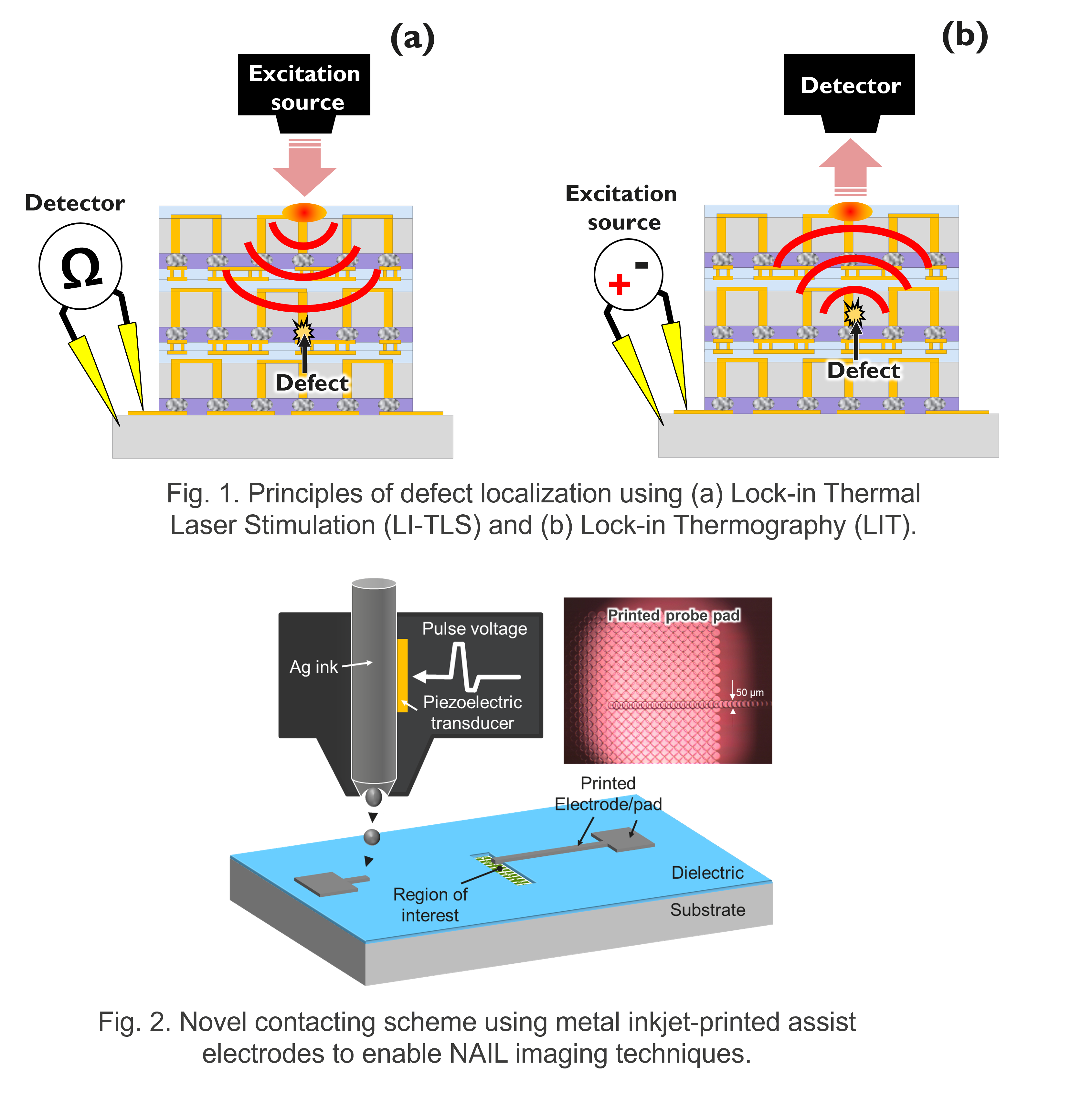
In this context, thermal-based techniques merge as a practical solution for accessing fault information in regions beyond the reach of optical methods. At imec, a novel lock-in thermal laser stimulation (LI-TLS, Fig. 1(a)) technique has recently been introduced [2], enabling localized thermal excitation and detection of fault signatures even in optically inaccessible regions. In parallel, an enhanced lock-in thermography (LIT, Fig.1 (b)) method has also been developed [3], offering improved sensitivity and spatial resolution. To enable the effective use of these techniques, new sample preparation methodologies will need to be investigated and developed. For example, metal inkjet printing of redistribution layers (Fig. 2), may enable the use of numerical aperture increasing lens (NAIL) techniques improving thermal imaging access and resolution [4].
This PhD project, in collaboration with KU Leuven, aims to further develop and refine these thermal techniques and sample preparation methods to meet the FA demands of future technology nodes.
Objectives
- Advance LI-TLS and LIT techniques for fault localization in 3D and nanoscale semiconductor devices.
- Develop high-throughput sample preparation strategies to enable thermal imaging access, including metal inkjet printing for redistribution layers.
- Perform thermal simulations to understand wave propagation in complex chip structures.
- Integrate AI-based models to improve fault detection accuracy and automate analysis.
- Validate methodologies on representative advanced node devices and packages.
The ideal candidate for this PhD project should have:
- Hands-on experimental skills, preferably in semiconductor device characterization.
- Proficiency in programming, with interest in data analysis and automation.
- A strong interest in physics.
- Interest in thermal and mechanical modelling
- Willingness to engage in interdisciplinary work
[1] https://www.imec-int.com/en/imec-magazine/imec-magazine-september-2017/new-technique-localizes-defects-in-3d-chips
[2] Jacobs, K.J.P., et al., “Lock-in thermal laser stimulation for non-destructive failure localization in 3-D devices”, Microelectronics Reliability, Vol. 76-77 (2017), Pages 188-193
[3] Sharma, A.M.R., Jacobs, K.J.P., Coenen, D. et al. Enhanced Infrared Imaging for Die-Level Fault Isolation Using Lock-In Thermography. J Fail. Anal. and Preven. 24, 2129–2141 (2024). https://doi.org/10.1007/s11668-024-02000-x
[4] Jacobs, K.J.P. Inkjet-printed electrical interconnects for high resolution integrated circuit diagnostics. Commun Eng 2, 21 (2023). https://doi.org/10.1038/s44172-023-00073-4
Required background: Engineering Technology, Engineering Science, Physics
Type of work: 60% experimental, 30% modelling/simulation, 10% literature
Supervisor: Houman Zahedmanesh
Co-supervisor: Kristof J.P. Jacobs
Daily advisor: Kristof J.P. Jacobs
The reference code for this position is 2026-153. Mention this reference code on your application form.