3D integration
The three-dimensional stacking of ICs is one way to further extend IC scaling. Imec explores different paths for such 3D integration.
One way to further scale ICs and add more functionality per area, is to integrate circuits on top of each other, leveraging 2.5D or 3D connectivity. Additionally, this may help solve a number of other challenges:
- Provide shorter paths between the processor and its memory, helping to break down the memory wall.
- Boost functionality in ICs that are limited in size.
- Improve the yield for large, complex systems.
3D integration is also a way to combine heterogeneous subsystems, i.e. dies made from different technologies. As SoCs are becoming increasingly more heterogeneous, the different functions on a chip (logic, memory, I/O interfaces, analog, ...) need not come from a single CMOS technology. It may be more advantageous to use different process technologies for subsystems, for example to optimize the design costs and yield. This evolution also answers the needs for more IC diversification and customization.
Imec’s aim is to help its partners attain all the benefits of 3D integration and SoC-level design. To do so, we’re working on a whole range of 3D enablers, some of them close to production, others still farther out.
In close collaboration with the ESD Association, imec also investigates the development of 3D-specific ESD protection strategies.

3D integration through die-to-wafer bonding
Imec is pushing the boundaries of what is physically possible for die-to-wafer bonding. We have, for example, demonstrated microbump interconnects with a record-low pitch. Such high-density connections bring about the full potential of through-Si-via technology. They allow 3D interconnect densities between dies or between dies and a silicon interposer that are more than sixteen times higher than the state of the art.

Direct bonding of dies to silicon is also possible using hybrid copper bonding. We are developing die-to-wafer hybrid bonding with pitches down to 2µm and high-tolerance pick-and-place accuracy, using what we learned in wafer-to-wafer hybrid bonding.

Cross-section TEM image of a die-to-wafer hybrid bonded test vehicle with 2µm bond pad pitch.
3D integration through wafer-to-wafer stacking
For high-density wafer-to-wafer stacking, we are working towards hybrid bonding with ultra-low interconnect pitches, currently aiming at 500nm pitch interconnects.
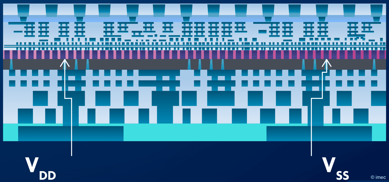
Wafer-to-wafer bonding also allows for extreme thinning of Si substrates and the realization of connections through the silicon in the 100nm range. These nano-vias allow for direct power delivery to the logic devices from the wafer’s back side, freeing-up space for wiring on the front side.
Explore this longread on backside power delivery
Such high-density wafer-level packaging technologies will boost the integration of heterogeneous systems in a small footprint. To help enable this, we work on new wafer reconstruction techniques (singulated devices, reconfigured in a wafer format) as well as high-density redistribution (RDL) technologies with dimensions of wires in the micrometer range and high-density through-package-via technologies.
Want to know more about imec’s 3D integration research?