Exploring single-bit domain wall device for next generation spintronics memory
PhD - Leuven | More than two weeks ago
With the increasing demand for data storage, the present charge-based memory technologies are reaching their fundamental limits due to their poor reliability and volatile nature. Spintronic devices, leveraging spin's degree of freedom, offers a promising solution thanks to their non-volatility, fast processing, and higher integration capabilities.
Spintronics has already been instrumental in various storage technologies, from hard disk drive read heads to Magnetic Random-Access Memory (MRAM). The heart of MRAM technology lies in the Magnetic Tunnel Junction (MTJ), comprising an oxide tunnel barrier between two ferromagnetic layers. In Spin-Transfer-Torque MRAM (STT-MRAM), data is read by the Tunnelling Magnetoresistance (TMR) effect and written by passing a current through the oxide tunnel barrier to switch magnetization. While mature, STT-MRAM suffers from writing scheme due to degradation of tunneling barrier. To tackle these challenges, Spin-Orbit Torque MRAM (SOT-MRAM) has been proposed. In this concept, charge-spin conversion in an adjacent heavy metal switches the magnetization of the storage layer. The separate writing and reading path in SOT-MRAM offers sub-ns writing speeds and improved reliability. Although SOT-MRAM research has made significant advancements, its widespread adoption is limited by high switching current and reliable approaches for field-free switching operation. These challenges are still the subject of intensive research.
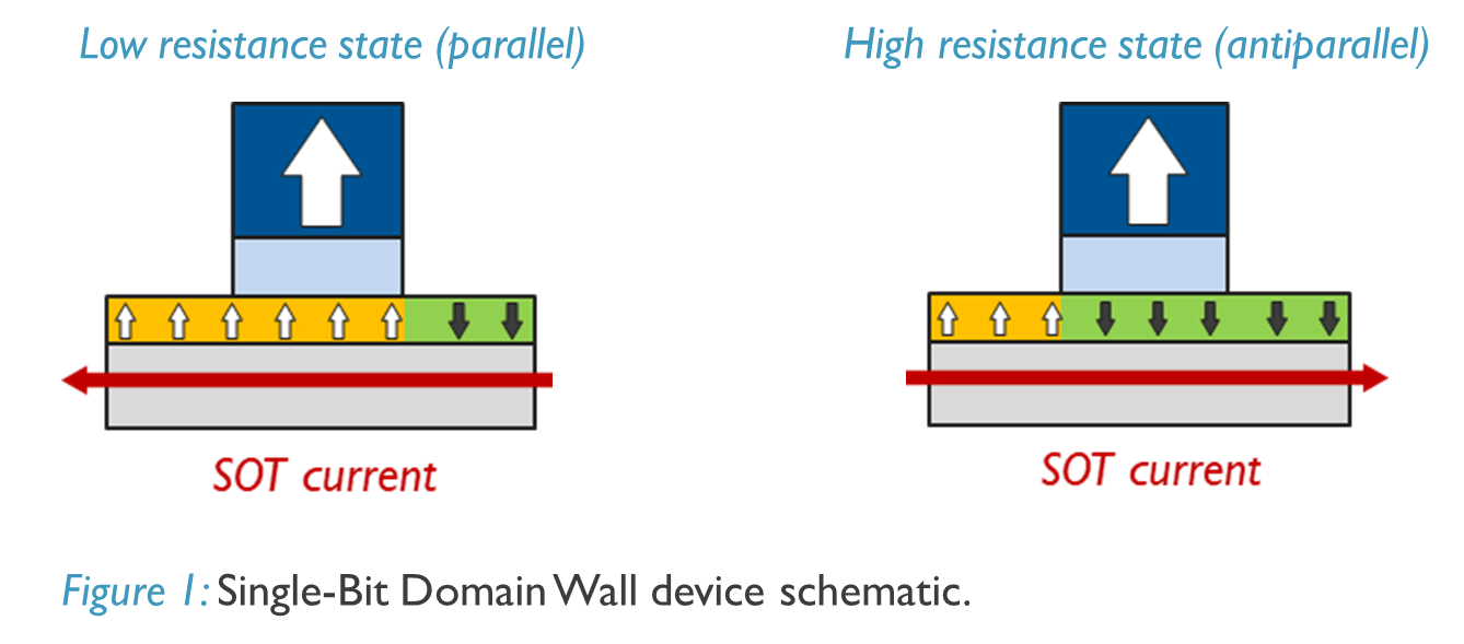
To overcome these issues, single-bit domain wall (DW) devices have been proposed. In these devices, the storage layer extends beyond the MTJ with information encoded by the position of a DW within this extended region [1]. Placing the DW at either edge of the MTJ leads to a distinct resistance state, thereby representing the two binary states (Fig. 1). The device is promising to reduce switching current, since moving a DW requires an order of magnitude less current than switching the full free layer, as in conventional SOT-MRAM devices. Furthermore, DW devices do not rely on an external magnetic field, providing a field-free alternative with improved scalability.
At imec, we have recently demonstrated the full electrical control of nanoscale DWs, employing MTJs as read and write components. This achievement is an important proof-of-concept as it demonstrates a practical way to manipulate DWs at nanoscale devices [2]. As a PhD candidate, you will build on this foundation to explore the physics of DW motion, optimize device designs, and contribute to making DW-based memory a realistic technology for the future memory.
The work will involve the design and fabrication of nanoscale test structures in imec’s state-of-the-art laboratory, combined with advanced electrical and magnetic imaging characterization techniques. The experimental investigation will be complemented by micromagnetic simulations using tools such as OOMMF and MuMax, enabling a comprehensive understanding of DW behaviours under various confinement schemes.
References
[1] S. -H. Yang, C. Garg, T. Phung, C. Rettner and B. Hughes, "Spin-Orbit Torque Driven One-Bit Magnetic Racetrack Devices - Memory and Neuromorphic Applications," 2019 International Symposium on VLSI Technology, Systems and Application (VLSI-TSA), Hsinchu, Taiwan, 2019, pp. 1-2. (https://ieeexplore.ieee.org/document/8804677)
[2] Imec brings magnetic domain wall devices closer to industrial reality. Imec. (https://www.imec-int.com/en/articles/imec-brings-magnetic-domain-wall-devices-closer-industrial-reality)
[3] About the NanoIC pilot line. from (https://www.nanoic-project.eu/en/abouthttps://www.nanoic-project.eu/en/about)
Required background: Physics, Nanomaterials and Nanotechnology, Electrical Engineering, Engineering Science
Type of work: 10% literature study, 30% modeling, 60% experimental analysis
Supervisor: Kristiaan Temst
Co-supervisor: Van Dai Nguyen
Daily advisor: Daniele Narducci
The reference code for this position is 2026-075. Mention this reference code on your application form.