International recognition and impact
With the different chips act initiatives in Europe, the USA and Asia solidifying over the past year, it has become evident that imec is being recognized by industry and policy makers as a critical contributor in the global semiconductor ecosystem. Serving as a testament to our conviction that strength lies in unity within the chip industry, we have extended existing partnerships and engaged in new collaborations across the globe in the past year, some of which we will highlight below.
We announced together with ASML our joint commitment to install ASML’s full suite of advanced lithography and metrology equipment in our pilot line in Leuven, technology that is crucial for developing high-performance, energy-efficient chips.
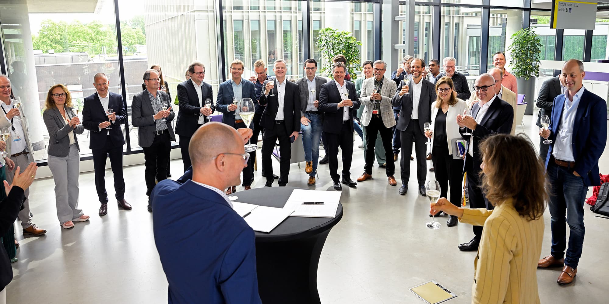
In July 2023, the Flemish government committed to match up to 750M euro the ambitions of the EU CHIPS ACT if the imec cleanroom is selected as one of the pilot lines under the Chips for Europe initiative. President of the EU Ursula Von Der Leyen underscored the EU ambitions with a visit to imec in the presence of Belgian Prime Minister A. De Croo, Flemish Minister-President J. Jambon, Flemish Minister of innovation J. Brouns and Peter Wennink, ASML CEO. And on November 30, commissioner Thierry Breton announced that EU CHIPS ACT funds for the various pilot lines, including a sub-2nm system-on-chip pilot line were approved, and calls are open. The commitment of Flanders and the EU will enable imec to remain world-leading in advanced nanoelectronics R&D.

Visit of President of the EU U. Von Der Leyen, Belgian Prime Minister A. De Croo, Flemish Minister-President J. Jambon, Flemish Minister of innovation J. Brouns and Peter Wennink, ASML CEO.
We also strengthened ties on a global scale. In the USA, we opened a joint R&D Lab with Purdue University (Indiana) and signed an MoU with University of Michigan, two of the world’s most respected universities, aiming at joint cutting-edge semiconductor R&D.
Another 2023 highlight was Rapidus, Japan’s newly founded chip manufacturer, joining our Core Partner Program, aiming at leveraging our leadership to reclaim Japan’s dominant position in the worldwide semiconductor ecosystem.
Advancing Moore’s Law beyond 2nm technology
Our SSTS program, attracting stakeholders from across the semiconductor industry to jointly develop strategies to control the ecological impact of the IC value chain, introduced the imec.netzero model that assesses manufacturing choices, identifies high-impact areas, and projects the future. We presented the first quantitative assessments from our model, revealing fluorinated etch gases, hydrogen and water consumption, and EUV throughput as high-impact areas of advanced patterning. We also presented a first life cycle assessment (LCA) of logic technology nodes (N28 to A14), showing a detailed breakdown analysis of the total emissions.
And we released a public version of our imec.netzero web application. This public version offers designers, academics and policy makers a high-level tool to make life cycle assessments and study the environmental impact of ICT.
From our memory program, we presented an improved memory window of the 3D trench unit cell, a prerequisite to realizing next-gen trench-based 3D NAND Flash. Also, we demonstrated for the first time multilevel, multiply-accumulate operations on IGZO-based 2-transistor-1-capacitor (2T1C) and 2T0C cells, paving the way to IGZO-based DRAM for energy- and area efficient analog in-memory computing. We demonstrated extremely scaled spin-orbit transfer magnetic random-access memory (SOT-MRAM) devices that achieve the best device performance ever published, bringing non-volatile SOT-MRAM technology a step closer to last-level cache memory applications.
With our nano-interconnect program, we demonstrated conductor films on 300mm wafers with lower resistivity than Cu and Ru.
We upgraded our integrated silicon photonics (iSSIP) platform, demonstrating the co-integration of our high-quality silicon nitride waveguide technology with our silicon photonics platform without performance degradation of the high-bandwidth active devices.
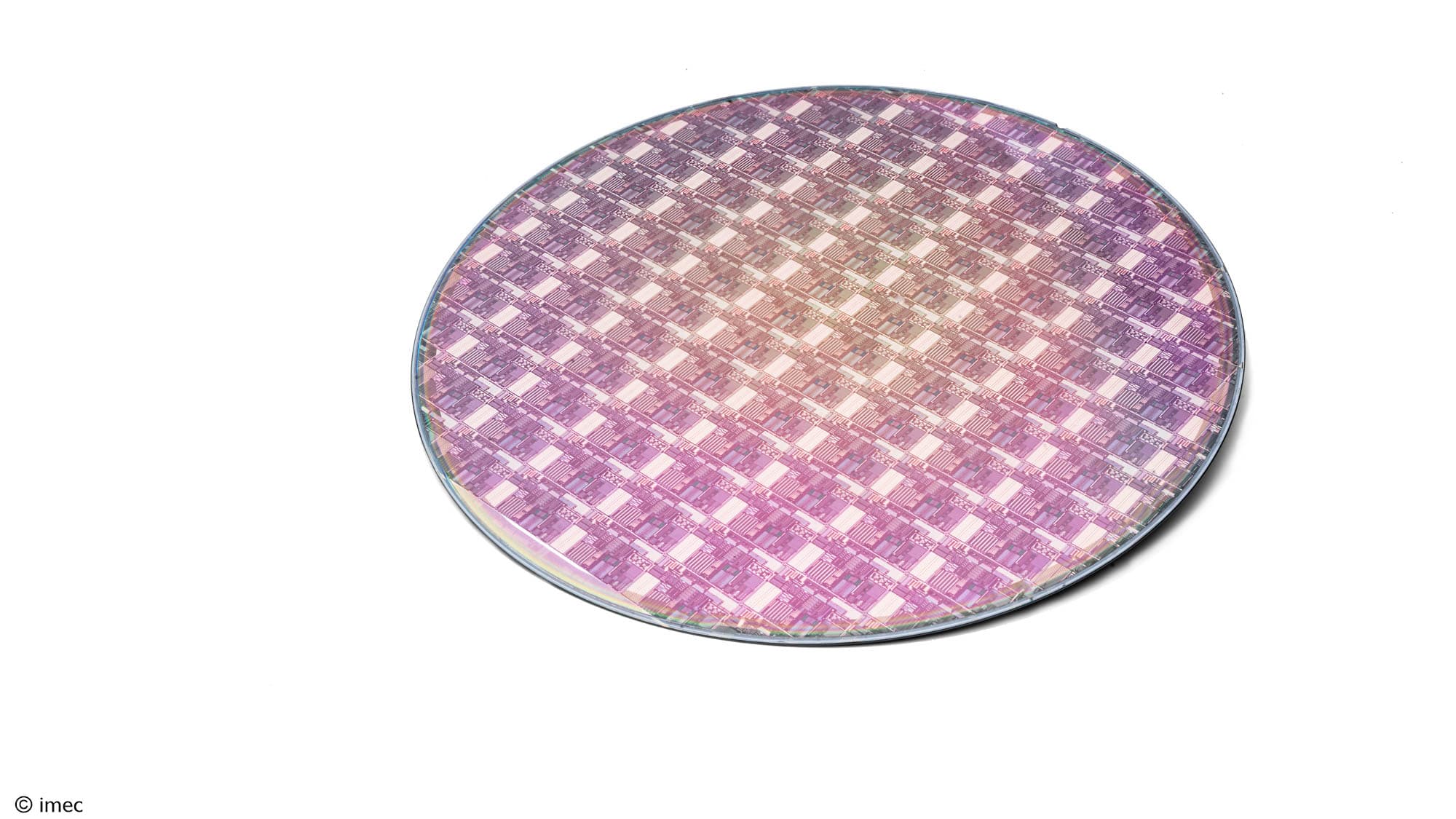
A 300mm wafer processed on imec’s iSiPP platform
In our 3D IC program, we reported important design and technology innovations in wafer-to-wafer hybrid bonding, achieving a record-low 3D interconnect pitch of 400nm, which is far below 1µm – today’s state of the art.
Quantum computing
In 2023, we demonstrated an ultra-low-power cryo-CMOS multiplexer that can operate at a record low temperature of 10mK.
Advancing connectivity
As the world becomes increasingly interconnected, the demand for seamless, high-speed, and reliable wired and wireless connectivity becomes paramount. At imec, we are tackling the technological challenges to meet the demands of our future communication infrastructure.
We presented an optical receiver that achieves a gross data rate of 200 Gbps. By combining a SiGe BiCMOS traveling-wave electronics integrated circuit and a silicon photonics germanium photodetector, we addressed both speed and scalability, two prerequisites if we want to meet exploding data-rate needs for next-generation high-speed wireline communication.

Close-up picture of imec’s SiGe BiCMOS optical receiver that achieves a gross data rate of 200 Gbps
On the wireless connectivity front, our GaN-on-Si MISHEMT technology has come on par with GaN-on-SiC device technology in terms of performance, while the adoption of the Si substrate provides a major cost advantage for industrial manufacturing.
Sense and actuate
Leveraging the exceptional capability of semiconductor technology to downscale prices and form factors, we are developing a wide range of sensors and actuator technologies enabling new applications in domains such as life sciences, agrifood, infotainment, mobility, etc.
We integrated a thin-film pinned photodiode into superior short-wave-infrared imaging sensors. With this game-changing achievement, we unlocked the superior absorption qualities of thin-film imagers in infrared imaging.

Imec's pinned photodiode structure integrated in thin-film image sensors
And, at IEDM 2023, we presented a fundamentally new way to render colors at sub-micron pixel sizes. The technology, which was one of the IEDM 2023 highlights, is poised to elevate high-end camera performance, delivering higher signal-to-noise ratio, enhanced color quality with unprecedented spatial resolution.
Semiconductor and digital technologies boosting sustainable innovation
Towards sustainable mobility
As a global leader in advanced 2.5D and 3D system-on-chip integration R&D, imec is spearheading a chiplet standardization initiative with the automotive ecosystem, to enhance collaboration and stimulate innovation in chiplets for automotive applications. In 2023, we organized two well-attended workshops on chiplet standardization, hosting an impressive representation across the automotive ecosystem, to discuss chiplets and how to jointly tackle their challenges.
We are also developing communication technologies for connected sensors in future cars. In 2023, we presented a novel ultra-wideband (UWB) transceiver that combines best-ranging precision with record-low power consumption. It paves the way for a variety of innovative (automotive) applications. One use case includes the creation of UWB radar-on-chip systems for in-cabin (child) presence detection, and driver monitoring.

Imec’s pioneering IEEE 802.15.4z compliant impulse radio (IR) ultra-wideband (UWB) transceiver for high-precision ranging.
Moreover, we leveraged our advanced semiconductor packaging expertise to develop, together with AT&S, a low-loss, low-cost and mass-manufacturable PCB with embedded chip and waveguides. The innovative approach lays the foundation for next-gen D-Band applications: compact, cost-efficient, and high-performance 140 GHz radar & 6G mobile communication systems.
Better healthcare at lower cost
Another area where we have significant impact through our expertise in nanoelectronics and digital technology is healthcare. By developing technology for next-generation health solutions we pave the way to more personalized precision medicine for better prevention, diagnosis or cure.
In 2023, we joined forces with the University Hospital of Leuven (UZ Leuven) to realize a compact set-up of our SNAPSCAN VNIR 150 hyperspectral camera on a standard OR-approved surgical microscope. The first intraoperative pilot tests at the hospital generated accurate clinical data, showing a promising path to the in-vivo detection of low-grade gliomas (a group of slow-growing brain tumors).
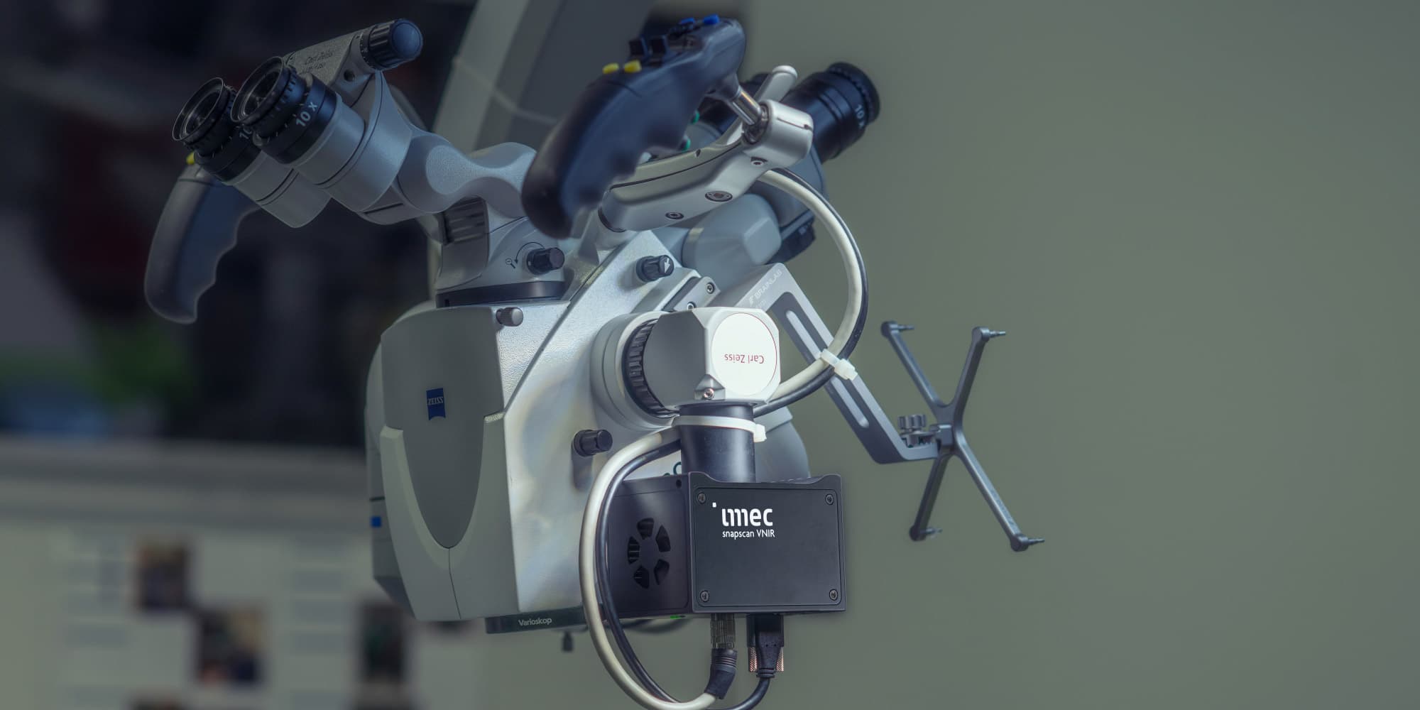
Imec's snapscan VNIR 150 camera mounted on a surgical microscope
We demonstrated, for the first time, a flat-panel-display-compatible ultrasound platform for large-area and curved surface applications. The achievement paves the way for complex ultrasound applications on curved surfaces, revolutionizing medical imaging and monitoring. Together with Pulsify Medical we are integrating the technology into a proof-of-concept for non-invasive, physician-free cardiac monitoring.
In 2023, our Neuropixels probe was for the first time demonstrated as a research tool to study human neurophysiology in the operating room. Imec researchers were co-authors in the Nature paper that reported these ground-breaking findings.
At IEDM 2023, we presented a dual-wavelength neural probe for simultaneous opto-stimulation and recording. It is the first time we combine both recording and stimulation into one implantable CMOS-based neural probe, paving the way to closed-loop solutions.
Decarbonization
In addition to our activities on Sustainable Semiconductor Technologies and Systems, we collaborate within the EnergyVille framework alongside partners KU Leuven, VITO and UHasselt to advance sustainable energy technologies and smart energy systems. We added an industry-compatible ammonium salt treatment to our perovskite solar cell process, improving two interfaces of the perovskite cells that largely contribute to efficiency losses and instability of this type of solar cells. The treatment resulted in highly efficient, stable and scalable perovskite cells.
We joined forces with industry partners to successfully develop highly efficient solar cells integrated into curved solar panels for car roofs, resulting in an efficiency gain of six percent.
Together with Bekaert, in a project funded by ESA, we produced functional solar cells on 200mm wafers, starting from germanium foils of only a few tens of micrometers in thickness. This achievement is a breakthrough for space applications.
Imec venturing
Positioned at the heart of the global deep-tech ecosystem, through our proficiency in nanoelectronics and digital technologies, along with our extensive venturing experience, we are well-placed to guide startups to succesfull market introduction, from idea to development, prototyping, and commercial success.
We launched four new spin-offs in 2023. IoSA, is a new spin-off of UAntwerp and imec that develops an animal behavior monitoring tool for research, conservation, and agriculture purposes. Enfoil is a Hasselt University and imec spin-off that offers pliable, extremely robust solar panels of only a few millimeters thick that can be integrated on various surfaces. The solar panels are the result of years of scientific research. Axithra is a spin-off of imec and Ghent University that raised 10M Euro to develop a new drug measurement and monitoring technology for accurate assessment of drug concentrations in blood. It paves the way for personalized and faster care. And Specifix is a spin-off of UAntwerp and imec that is developing an AI-based tool to support orthopedic surgery. The AI tool visualizes how the skeletal structure can be reconstructed starting from the bone fragments after trauma. This should lead to a better outcome after surgery.
Our imec.istart program was ranked number one start-up accelerator linked to a university by UBI Global, a recognition for our leadership in supporting start-ups and spin-offs.