CMOS 2.0: a new trajectory for CMOS scaling
In 2024, imec introduced CMOS 2.0 as a new scaling paradigm to cope with the ever-increasing variety of computational needs associated with the diversification of applications [1,2,3]. With CMOS 2.0, a system-on-chip (SoC) is partitioned into different functional layers (or tiers) guided by system-technology co-optimization (STCO). Each of the functional layers is built using the technology option that most closely matches the constraints of the functionality.
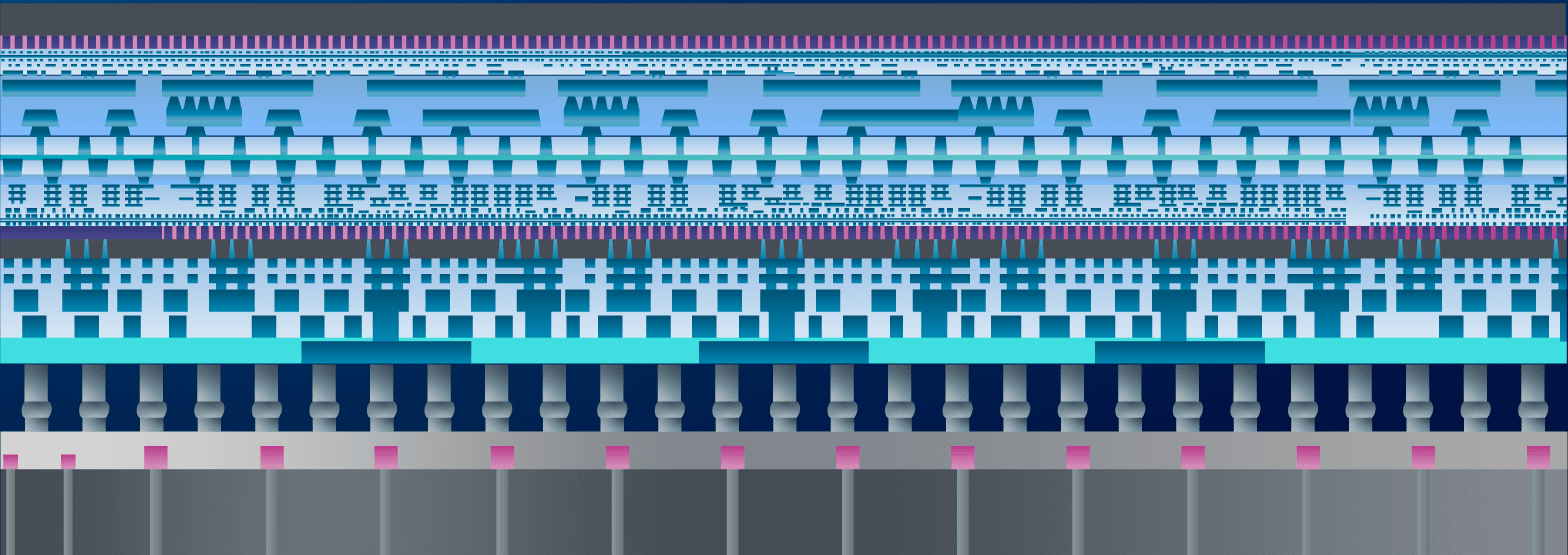
Advanced 3D interconnect technologies reconnect the heterogeneous tiers of the SoC. This is reminiscent of an evolution that has already made its way into commercial compute products: think about the 3D stacking of an SRAM chip on top of a processor. But what marks the CMOS 2.0 approach is that the heterogeneity is brought inside the SoC itself. Depending on the needs of the application, CMOS 2.0 envisions even splitting the logic part of the SoC into a high-drive logic layer (optimized for bandwidth and performance) and a high-density logic layer (optimized for logic density and performance/Watt). The high-density layer can be fabricated using the most advanced technologies, including the most scaled transistor architecture.
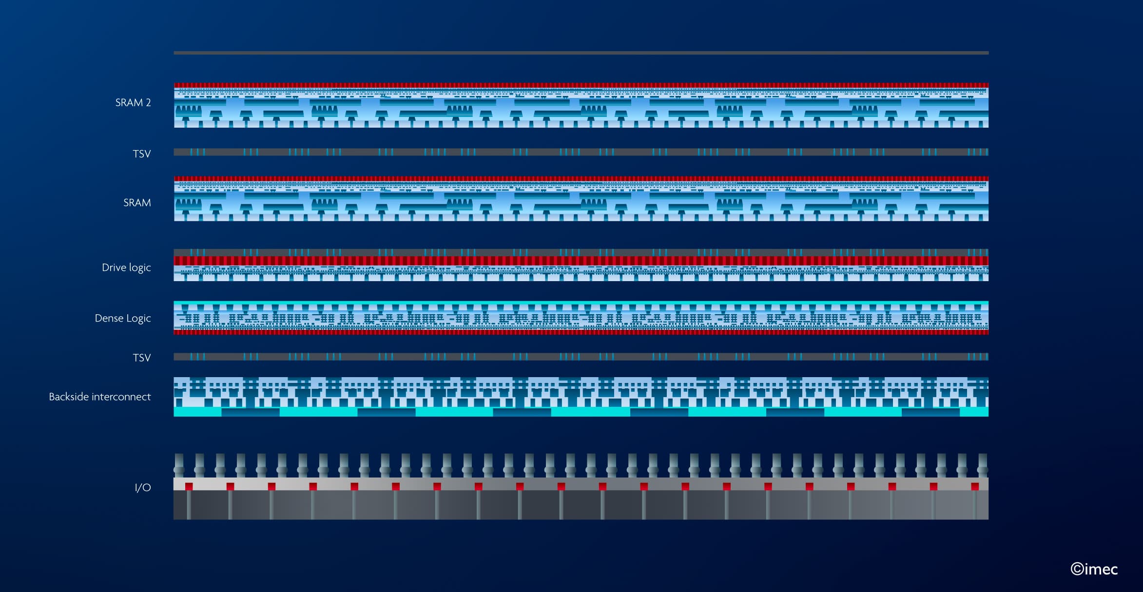
Figure 1: Example of a possible partitioning of a SoC in the CMOS 2.0 era.
Do you want regular updates on imec’s semiconductor research?
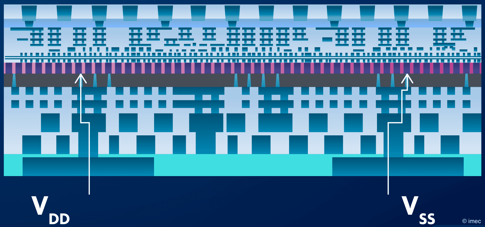
Another key feature is a backside power delivery network (BSPDN): part of the active devices is powered from the wafer’s backside rather than through conventional frontside power delivery schemes. As such, extreme back-end-of-line (BEOL) pitch patterning will be possible in the tier’s frontside without the constraint of voltage drop on the power supplies.
Basically, in this approach we have modified the device wafer in a very thin front-end-of-line (FEOL) active device layer, with on one side (the original ‘frontside’) a dense back-end-of-line (BEOL) signal routing layer stack and on the other side (the original ‘backside’ but now the new frontside) the power supply and external I/O connections. It is also possible to stack multiple of such thin device layers with dense interconnects on each side. Each layer may integrate different types of devices, e.g., logic, memory, electrostatic discharge (ESD) protection devices, voltage regulating circuits... We call this dense 3D stacking of device layers CMOS 2.0.
With this approach to system scaling, chip design and manufacturing move away from the general-purpose CMOS technology platform that has served the semiconductor industry for decades but struggles to adequately address the growing and diversifying compute demands. This approach helps solve compute system scaling bottlenecks, bringing value to every player in the semiconductor ecosystem – including system and fabless companies.
3D interconnection and backside technologies: foundational to CMOS 2.0
CMOS 2.0 relies on all semiconductor innovations of the past, including logic device scaling, memory density scaling, advanced lithography, 3D integration, and BSPDN technology. But the concept can only now become a reality thanks to recent breakthroughs in 3D interconnection and backside technologies. Wafer-to-wafer hybrid bonding, for example, starts to offer sub-µm interconnect pitch connectivity. It can as such provide an interconnect density matching the last metal layers of the BEOL – key to enable logic-on-logic or memory-on-logic tier stacking with hybrid bonding connections. Backside power delivery technology is expected to evolve to an even finer granularity level with the enablement of direct access to transistor terminals. This capability, although initially targeted for power connections, opens the possibility for fine-grain signal connectivity to also migrate to the backside. In this way any device technology layer will become suspended between 2 independent interconnect stacks.
The combination of fine-pitch bonding and fine-grain backside processing (Figure 2) is foundational to enable the vision of CMOS 2.0 illustrated in Figure 1.
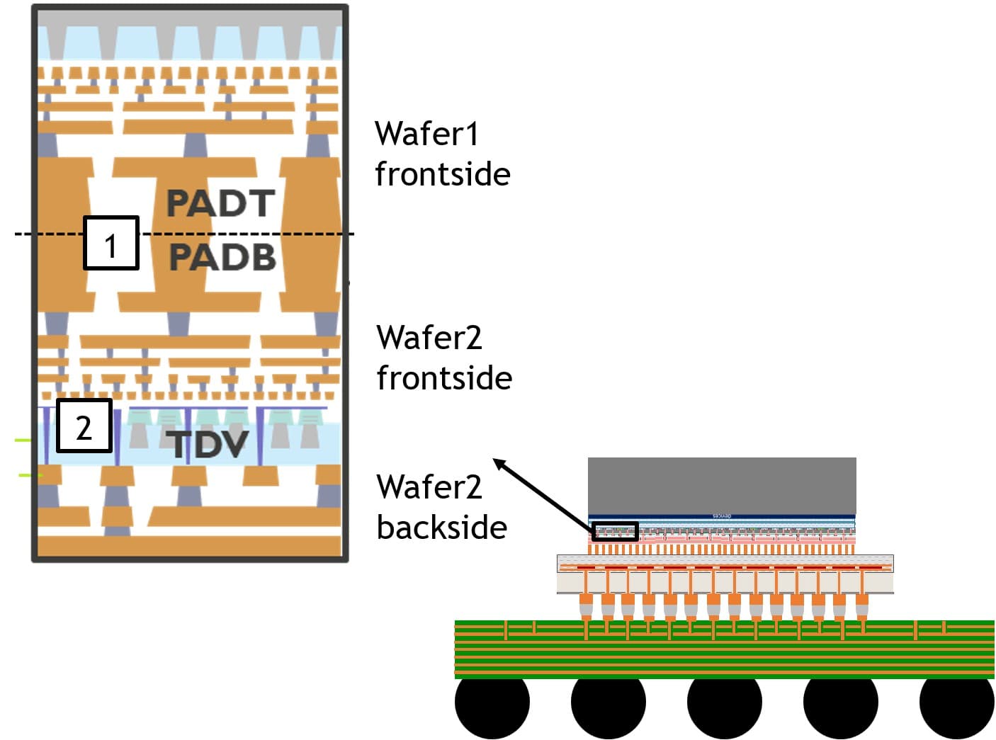
Figure 2 – Schematic illustration of high-density face-to-face hybrid bonding connections and a backside high-density connectivity network (as presented at 2025 VLSI [4]). (PADT =top pad; PADB = bottom pad; TDV = through-dielectric via.)
At the 2025 VLSI conference, imec reported progress in wafer-to-wafer hybrid bonding and backside vias, two 3D integration technologies underpinning the realization of CMOS 2.0 [4]. These technologies lay the foundation for designing new system architectures around the CMOS 2.0 vision – guided by STCO – in which BSPDNs will play a central role. Also at 2025 VLSI, imec researchers highlighted the power-performance-area-cost (PPAC) benefits that such BSPDNs can bring to advanced system architectures [5].
Wafer-to-wafer hybrid bonding towards 250nm pitch: a roadmap view
A large variety of 3D interconnection technologies have been developed over the years, spanning a broad range of interconnect pitches and serving different applications needs. Of all these technologies, wafer-to-wafer hybrid bonding is best suited to provide the 3D interconnect pitches and densities required for memory/logic-on-logic tier stacking in a CMOS 2.0 context. Wafer-to-wafer bonded Cu pads offer short and direct low-resistive connections from one tier to the other. At scaled pitch, the wafer-level connections can deliver a high bandwidth density as well as reduced energy per bit during signal transmission.
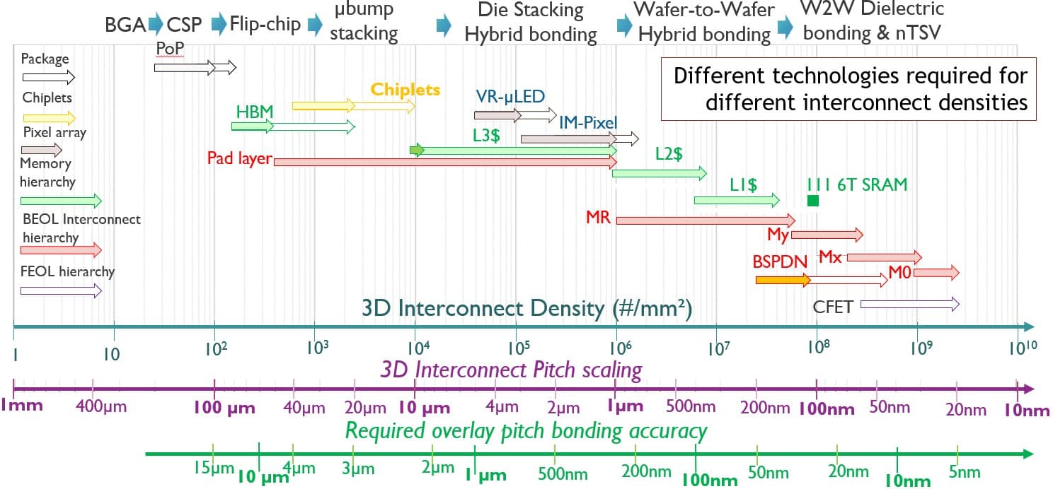
Figure 3 – Imec’s 3D interconnect technology scaling roadmap, showing the different technologies required for different interconnect densities. (BGA=ball grid array; CSP=chip scale package; W2W = wafer-to-wafer; Mx, My and MR represent the BEOL interconnect hierarchy).
The classical wafer-to-wafer hybrid bonding process flow
A classical hybrid bonding process (Figure 4) starts from two fully processed 300mm wafers, with completed front-end-of-line (FEOL) and BEOL (see also Figure 2). The first part of the flow resembles an on-chip BEOL damascene process, where small cavities are etched into the bonding dielectric – for which SiO2 is predominantly used. The cavities are filled with barrier metal, seed, and Cu. This is followed by a chemical mechanical polishing (CMP) step optimized for high across-wafer uniformity to produce extremely flat dielectric surfaces while achieving a controlled few nanometers of recess for the Cu pads. After accurate alignment, the actual bonding of the two wafers is performed at room temperature by bringing the wafers into contact at the center of the wafer. The polished wafer surfaces adherence results in a strong wafer-to-wafer attraction, resulting in a bonding wave, closing the wafer-to-wafer gap from the center to the edge. After this room temperature bonding step, the wafers are annealed at higher temperatures to obtain a permanent dielectric-to-dielectric and Cu-to-Cu bond.
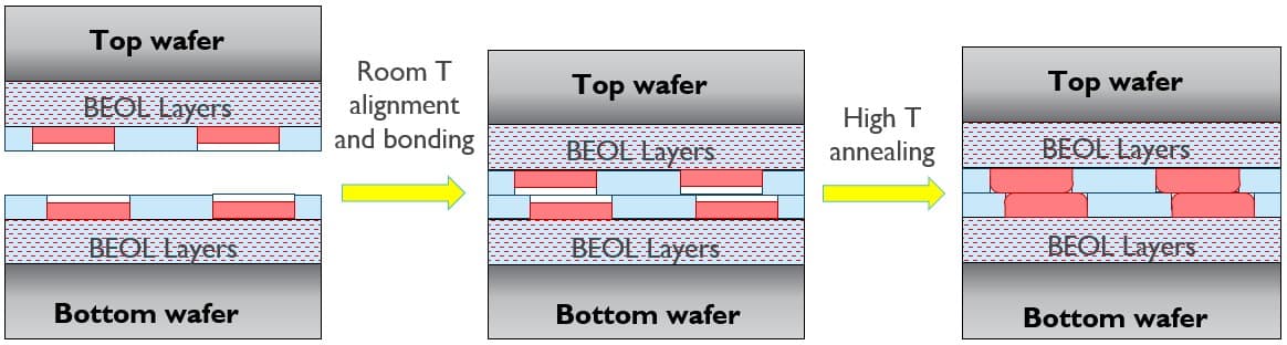
Figure 4 - The classical wafer-to-wafer hybrid bonding process flow.
Reliable 400nm pitch wafer-to-wafer connections
At IEDM 2023, imec demonstrated reliable 400nm pitch wafer-to-wafer connections at high yield, a significant improvement over the 1µm pitch connections used in industrial wafer-to-wafer bonding processes [6]. This leap in interconnect pitch was enabled by several process flow improvements, including enhanced control of the wafers’ surface topology and the use of SiCN as the bonding dielectric. SiCN was found to offer better bonding strength and scalability than conventional SiO2.
Pushing the hybrid wafer-to-wafer bonding roadmap towards 200nm pitch
Whenever we go deeper in the system hierarchy – ultimately splitting the logic part into specialized logic layers – bonding pitches below 400nm will be needed, driving the wafer-to-wafer hybrid bonding roadmap towards 200nm pitch. But as the pitch continues to scale, so do the requirements for the bonding overlay between two Cu pads. In general, the overlay accuracy of the bonding process corresponds to one fourth of the pitch, translating into an overlay as small as 50nm for a 200nm pitch bonding process. Achieving this high level of accuracy at 300mm wafer scale is today’s biggest challenge to achieve higher interconnect densities.
To continue the roadmap, imec researchers work towards a more fundamental understanding of the bonding process, and the factors that interfere with the high level of overlay accuracy. It is well known that during bonding, the two wafers get easily deformed and distorted, hindering precise overlay between Cu pads. The team found through simulations that the bonding wave that occurs when the two wafers adhere, does not propagate uniformly – a phenomenon believed to underlie wafer deformation. These insights can help build models that allow us to predict how much the wafers deform and to eventually finetune the bonding recipes.
This knowledge can also help to improve overlay accuracy in another way: designers can shift the Cu pads in the pattern design before the actual wafer bonding. These pre-bond litho corrections allowed imec to achieve wafer-to-wafer hybrid bonding at 300nm pitch with overlay error less than 25nm for 95% of the dies, using today’s most advanced bonder tools.
At VLSI 2025 [4], imec researchers showed the feasibility to further extend the wafer-to-wafer hybrid bonding roadmap to an unprecedented 250nm pitch. However, to achieve the required overlay accuracy at industry-relevant yield over the full 300mm wafer, next-generation bonding equipment will be needed. Imec continues to work with its ecosystem of tool suppliers towards that ambitious goal.
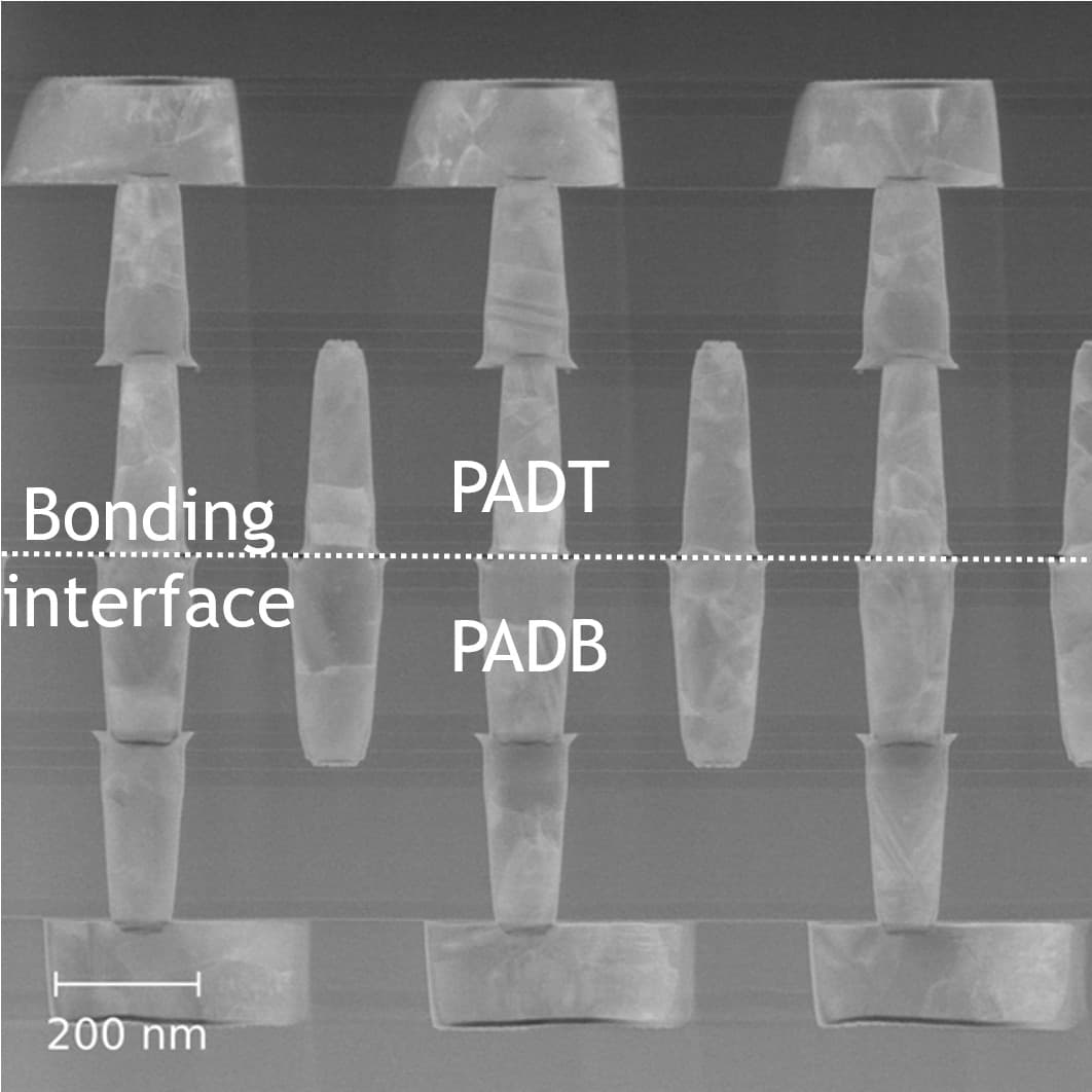
Figure 5 – TEM of daisy chains (with bonded top (PADT) and bottom (PADB) pads of unequal size) on a 250nm hexagonal pad grid (as presented at VLSI 2025 [4]).
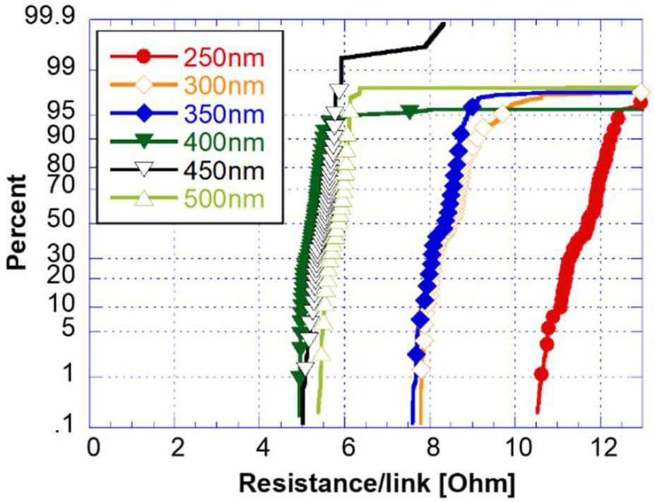
Figure 6 – Electrical yield on hybrid bonded daisy chains as a function of pad pitch for unequal pad sizes (as presented at 2025 VLSI [4]).
Connecting the tier’s front and backside metals with nano-through-silicon vias
In CMOS 2.0 implementations, the stacking of tiers will be much more complex than in today’s industrial hybrid bonding cases. Not two, but multiple tiers will be stacked on top of each other. Most of the tiers will have metal lines on both sides – on their front- as well as their backside – with an active layer (e.g., memory or logic) in between. Part of the backside metal lines may be used to power the active devices, as part of a broader BSPDN.
Enabling front-to-back connectivity with direct backside contacting and nano-through-silicon vias
Following this vision, tiers now have connections on both sides, with front- and backside metals connected to each other in a seamless way. This front-to-back connectivity can be realized with through-silicon vias (TSVs), at the granularity of logic or memory standard cell level. When going deeper in the system hierarchy, other front-to-back connections at finer interconnect pitch are needed, including direct backside contacting. This connectivity scheme can be used to directly connect the source/drain contact areas of advanced logic devices to the backside metal and is emerging in the logic roadmap of leading foundries.
Evolution in front-to-backside connectivity technologies must keep pace with the advancement of the wafer-to-wafer hybrid bonding roadmap, as to offer tight pitch connections on both sides of the wafer in a balanced way (see also Figure 2). But combining all these technologies also brings challenges. Increasingly more post-processing is required after the wafer-to-wafer bonding step, including wafer thinning (to support the fabrication of TSVs) and backside metal patterning. During the latter step, minimizing backside lithography distortion is crucial to ensure tight overlay between the backside metal lines and either the TSVs or source/drain contacts.
Backside through-dielectric vias with 20nm bottom diameter
At VLSI 2025, imec presented progress in its nanoTSV (nTSV) roadmap, showing backside vias with a diameter as small as 20nm, at 120nm pitch [4]. Vias with such a small diameter offer the benefit of consuming as little of the standard cell area as possible, but their fabrication requires extreme wafer thinning to ensure manageable aspect ratios.
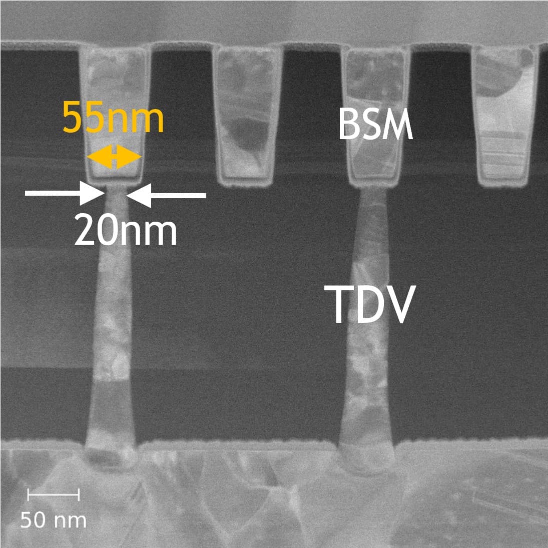
Figure 7 – TEM of frontside-to-backside connections using barrier-less Mo-filled TDVs with 20nm bottom diameter (as presented at 2025 VLSI [4]).
Imec’s roadmap offers several options for making nTSVs, including via-first, via-middle and via-last integration. In addition, vias can be made with circular or slit-shaped bottoms [7], trading overlay tolerance for area consumption. In the 2025 VLSI demonstration, vias were made using a via-first approach, meaning that the vias are already patterned within shallow-trench isolation (STI) features on the wafer frontside prior to wafer thinning. The resulting through-dielectric vias (TDVs, so called because these vias run through the STI dielectric) were filled with molybdenum (Mo). Mo can be implemented without a barrier and offers smaller resistance than conventional Cu or W metals – benefiting both area and performance.
Connecting front- and backside with high overlay accuracy
The layout of a typical test structure showed 15nm overlay margin between the 55nm wide backside metal lines and the 20nm wide circular bottom of the Mo TDVs. This overlay specification can be achieved using higher-order corrections per exposure in the backside metal lithography step, to compensate for the grid distortions from preceding wafer bonding and thinning steps.
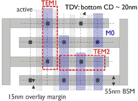
Figure 8 – Layout showing 15nm overlay margin between the bottom of the TDV and the 55nm wide backside metal (as presented at 2025 VLSI [4]). (TEM1 represents the TEM cut used in Figure 7.)
In all previously discussed connecting schemes, achieving high total overlay accuracy in hybrid bonding as well as minimizing backside lithography distortion are crucial targets that both rely on the bonding process and on the capabilities of next-generation bonding equipment.
Performance and area benefits of BSPDNs in always-on and in switched-domain designs
BSPDNs are another key feature of future CMOS 2.0 architectures. With a BSPDN, the entire power distribution network is moved to the wafer’s backside, where the power-delivering interconnects can be made larger and less resistant. BSPDNs can therefore significantly reduce supply-voltage (or IR) drops. This facilitates designers to maintain the 10 percent margin allowed for the unwanted power loss that occurs between the voltage regulator and the active devices. By decoupling the power delivery network from the signal network, BSPDNs also allow decongesting the BEOL in the wafer’s frontside, which can now be more efficiently designed for signal transport.
Imec pioneered the concept of BSPDN in 2019 and has meanwhile proposed several options for implementing BSPDNs [8]. Some major chip manufacturers have recently introduced the technology in their logic roadmap, and plan to offer commercial products with advanced processors relying on BSPDNs. The technology also shows promise for 3D SoC implementations, and benefits are expected for CMOS 2.0 architectures as well.
BSPDNs in always-on and switched-domain designs: performance and area improvement over frontside implementations
In the past, imec has demonstrated the PPAC merits that BSPDNs can bring at block level, for high-density as well as for high-drive logic use cases [8]. These benefits have been shown through design-technology co-optimization (DTCO) studies for always-on use cases, architectures where power (i.e., global VDD) is continuously delivered to the active devices.
At VLSI 2025, imec has also shown the benefits of implementing BSPDNs in switched-domain designs where blocks of standard cells are turned off for power management [5]. Switched-domain designs are realized by locally implementing power switches: devices that distribute power (local VDD) to the transistors locally and can turn groups of standard cells on and off when needed. These designs are typically used in power-constrained applications such as mobile phones.
Imec researchers compared the impact of using BSPDNs in switched-domain designs with traditional frontside PDN implementations. The study was performed through physical implementation of a mobile compute processor design in 2nm technology.
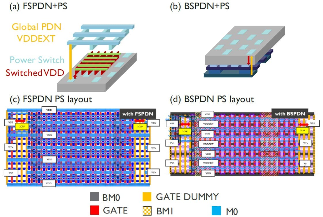
Figure 9 – (a-b) Power delivery of switched-domain designs with power switches placed in a checkboard pattern; (c-d) power switch layouts for frontside and backside PDNs (as presented at 2025 VLSI [5]). (VDDEXT=the always-on power; VDD=the switched power; PS=power switch.)
The BSPDN implementation resulted in improved performance as well as reduced area consumption compared to frontside PDN switched-domain designs. With a BSPDN, the IR drop could be significantly reduced (by 122mV). This allowed the BSPDN design to use fewer power switches and still manage an acceptable IR drop. The reduced amount of power switches takes up less core area space compared to frontside PDN implementations: a total 22 percent area reduction is achieved by using a BSPDN implementation.
Conclusion
With CMOS 2.0, a new scaling paradigm will unfold that can meet the growing diversification of compute applications. It relies on the stacking of functional tiers – each optimized using the most suited technology (node). Fine-grain backside processing as well as fine-pitch hybrid bonding are key to enable this vision. Recent advances in wafer-to-wafer hybrid bonding motivated by SRAM partitioning and backside technologies driven by power delivery optimization bring the CMOS 2.0 concept closer to reality, offering tier-to-tier connectivity at the granularity of logic and memory standard cells. These foundational technologies will make it possible to bring heterogeneity – central to current chiplet approaches – within the SoC itself, creating more options for compute system scaling.
This work has been enabled in part by the NanoIC pilot line. The acquisition and operation are jointly funded by the Chips Joint Undertaking, through the European Union’s Digital Europe (101183266) and Horizon Europe programs (101183277), as well as by the participating states Belgium (Flanders), France, Germany, Finland, Ireland and Romania. For more information, visit nanoic-project.eu.
As published in the July/August 2025 issue of Chip Scale Review

Want to know more?
[1] ‘CMOS 2.0: bringing heterogeneity inside the system-on-chip,’ imec Reading Room;
[2] ‘What is CMOS 2.0?,’ IEEE Spectrum, 2024;
[3] ‘The CMOS 2.0 revolution,’ Nature Reviews Electrical Engineering, 2024;
[4] ‘High-density wafer level connectivity using frontside hybrid bonding at 250nm pitch and backside through-dielectric vias at 120nm pitch after extreme wafer thinning,’ L. Witters et al., 2025 VLSI;
[5] ‘Backside power delivery for power switched designs in 2nm CMOS: IR drop and block-level power-performance-area benefits,’ Y. Zhou et al., 2025 VLSI;
[6] ‘Wafer-to-wafer hybrid bonding: pushing the boundaries to 400nm interconnect pitch,’ imec Reading Room;
[7] ‘Backside Power Delivery with relaxed overlay for backside patterning using extreme wafer thinning and Molybdenum-filled slit nano Through Silicon Vias,’ P. Zhao et al., 2024 VLSI;
[8] ‘Backside power delivery options: a DTCO study,’ imec Reading Room.