ESD induced failures in electronic products: a longtime concern
No doubt everyone has experienced in real life what an electrostatic discharge (ESD) is. When walking across a carpet and then touching a metal doorknob, for example. When that happens, charges of a few thousand Volt (V) and more, accumulated in the human body during walking, rapidly drain through the doorknob.
While humans are insensitive to discharges up to 3000V, electronic devices can already be damaged by discharges as low as 3V. All electronic products and technologies – be it at component or system level – can be affected by ESD events. These can occur at any point during manufacturing and assembly, and during transportation and use of the product. During assembly, for example, a chip can be damaged when it is mounted on a PCB or picked up by a tweezer with different electrostatic potential. During use, damage may occur when humans touch the in- and output pins of an IC device.
Characteristic for ESD events is their short duration, a feature that distinguishes them from comparable but longer-lasting electrical overstress (EOS) events. The ESD discharge happens in a very short timeframe (about 1ns or in the order of 200ns, depending on the type of the ESD event), with rise times of 200ps to 10ns. In this short period of time, excess currents in the order of 0.1 – 10A run through the IC and package, dissipating 10 – 100W of power. The chip itself can get damaged in the form of, e.g., metal interconnect burnout, gate oxide rupture or junction breakdown.
The impact of ESD on electronic devices cannot be overrated. Since technology nodes moved into the sub-micron regime, it has become the predominant failure cause. Industrial statistics suggest that today, almost 40% of the IC failures are related to EOS/ESD events, resulting in billions of dollars in losses annually to the industry. It is therefore not surprising that the semiconductor industry is betting heavily on reducing the number, severity, and impact of ESD events.
Measures to safeguard ICs: prevention and protection
A lot of effort is put into the prevention of ESD events within the environment – during manufacturing, assembly, and transportation of ICs. Manufacturing and assembly occur at tightly ESD-controlled facilities, where appropriate materials are being used, and personnel and equipment are properly grounded. These antistatic measures are continuously improved to ensure that, during the critical steps, as little as possible static charges build up and discharge.
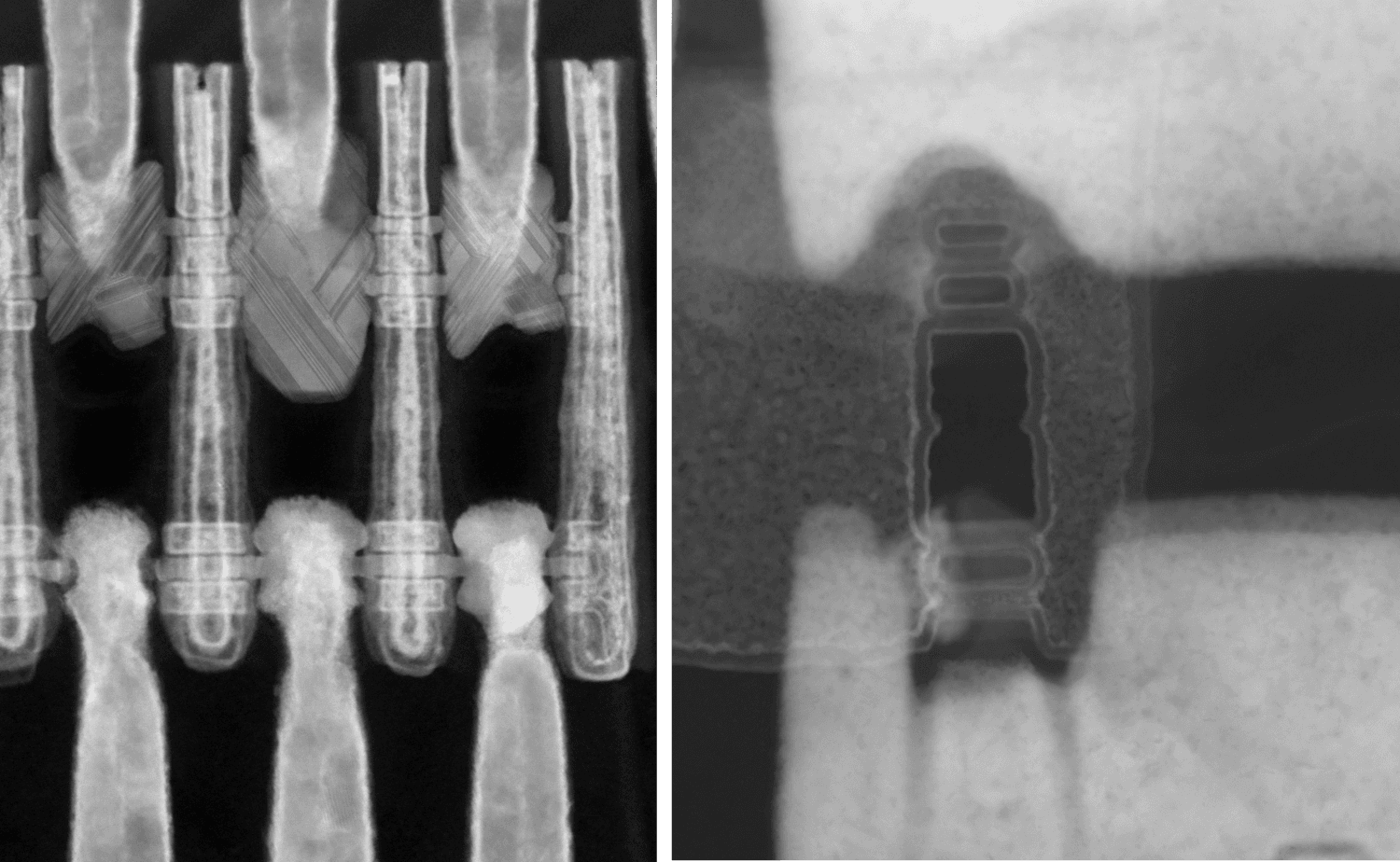
Figure 1 - Example of a technology for ESD prevention. The picture shows ESD events from an ESD gun to the metal handle of the tweezer. The tip of the tweezer is made of ‘ESD-dissipative’ material that suppresses fast ESD events.
Since prevention cannot exclude all ESD events, it is complemented with adding on- and off-chip protection circuitry. On-chip ESD protective circuits play a major role in shielding the chip’s power lines and ground, and the input and output interfaces (I/O) that communicate with the outside world. Whenever an ESD event hits the chip, the ESD circuits ensure a safe, low-resistive discharge path to the ground while limiting voltage to a safe level.
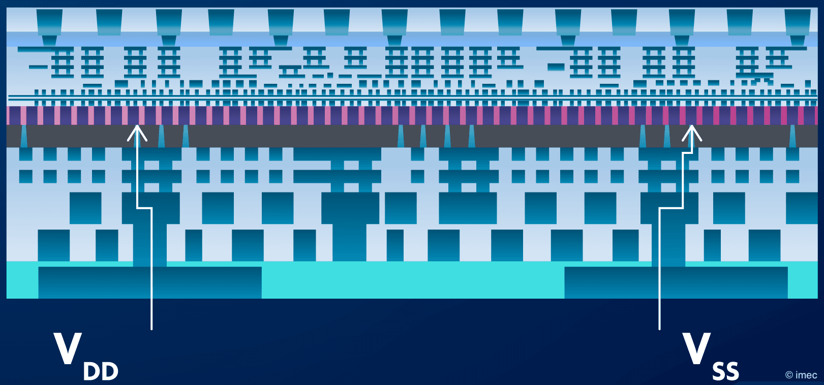
Figure 2 – Schematic illustration of on-chip ESD protection. ESD devices are implemented on all inputs and outputs, between power lines and ground, and between different power domains – if possible.
To measure the performance of the ESD protection devices, and to qualify the chip’s robustness to ESD events, the semiconductor industry relies on two standards that are representative of the most common ESD events. The human body model (HBM, about 200ns duration) standard, originally representing the discharge from a human-being to the device, today also includes discharges from other external objects within manufacturing and assembly lines. The charged device model (CDM, about 1ns duration), on the other hand, emulates what happens when the chip itself is charged and discharges to the environment. The I-V characteristics measured by applying transmission line pulse (TLP) stress and very fast TLP (VF-TLP) stress correspond the performance of the devices to HBM and CDM, respectively.
Today, the semiconductor industry typically requests 250V CDM as a spec for the most advanced technologies used in high-performance computing applications. For HBM, the spec depends on the functionality of the I/O pins. For general I/O and for power supply and ground lines, specs can reach 500V HBM and higher, while for high-speed I/O pins, around 100V is adopted. Adding ESD protection circuitry, however, adds to the cost of the electronic system, which makes companies sometimes opt for lower targets. The specs also differ from one application area to another. Automotive, for example, uses different standards and requires ESD robustness against a few thousand V to ensure people’s safety.
State-of-the-art ESD protection devices
Different types of ESD protection devices exist, and their selection is based on the nature of the circuit that needs protection. ESD diodes, both shallow trench isolation (STI) diodes and gated diodes, are the most widely used. They are structurally simple, and, when forward-biased, are considered one of the most effective protective elements, with low turn-on voltage, low on-resistance, and the ability to handle high ESD currents. They are used, for example, to protect the input pins of the IC. ESD diodes are often combined with power rail clamps in between power supply and ground to ensure low voltage levels. Besides diodes, grounded-gate NMOS (GGNMOS) devices are also popular in ESD designs. GGNMOS are off-state MOSFETs that discharge ESD current through a parasitic bipolar conduction mechanism.
Be it in the form of diodes or channel-based MOSFETs: all ESD devices have transistor-like structures that are fabricated during front-end-of-line (FEOL) processing of the chip. They typically leverage the same CMOS technologies used to build the chip’s core transistors. To efficiently discharge the excess currents to the ground and dissipate heat, most ESD protection circuits heavily rely on the thick Si substrate that resides within the chip’s backside.
Emerging technologies challenge ESD protection designs
The introduction of novel technologies in the semiconductor technology roadmap may bring along new ESD vulnerabilities worrying the semiconductor industry. To better describe upcoming requirements and define new standards, the chip industry therefore closely collaborates with the EOS/ESD Association in which imec is actively involved.
With CMOS scaling, the area margins for implementing ESD protection circuits are shrinking accordingly. Besides, the dimensional scaling of logic transistors may impact the performance of the ESD protection devices that are partly made in the same technology. A similar concern arises when new transistor architectures enter the roadmap. Think about the historical move from planar MOSFET to FinFET devices, the introduction of gate-all-around (GAA) FETs in the latest logic technology nodes, and the envisioned transition to complementary FET (CFET) devices. In monolithic SOCs, such transitions have already been shown to impact the protective capabilities of the ESD devices [1].
On top of that, system applications increasingly move to 3D stacked technologies, a trend that is booming thanks to the enormous potential offered by 2.5D and 3D chiplet technologies. From ESD perspective, a distinction is made between the external I/O interfaces that communicate to the outside world, and the internal I/Os that communicate between the dies or stacked modules. For external I/O, nothing really changes, as these circuits can still be electrostatically discharged to and from external objects or humans. Comparable HBM and CDM standards as defined for monolithic chips therefore remain valid. For the internal I/O interfaces, however, different standards apply. Once the external I/O ports are shielded, the main risk for damaging internal connections arises during stacking and assembly. Damage may occur, for example, when integrating an electrostatically charged chip onto a grounded 2.5D interposer. For the internal I/Os in 3D technologies, focus is therefore shifting to increased environmental control to prevent such discharges. Eventually, the goal is to eliminate the need for on-chip ESD devices to protect the internal interfaces in 3D designs.
Finally, in the design-technology co-optimization (DTCO) and system-technology co-optimization (STCO) scaling era, new scaling boosters (such as backside power delivery networks (BSPDNs)) and advanced 3D integration technologies (such as wafer-to-wafer hybrid bonding) are increasingly being used to unlock major system scaling bottlenecks. Typical of these technologies is the thinning of the Si substrates to a few hundred nm to enable through-Si-via (TSV) interconnects with reasonable aspect ratios. This raises concerns, as most of the conventional ESD protection circuits heavily rely on thick Si substrates to dissipate heat and discharge efficiently.

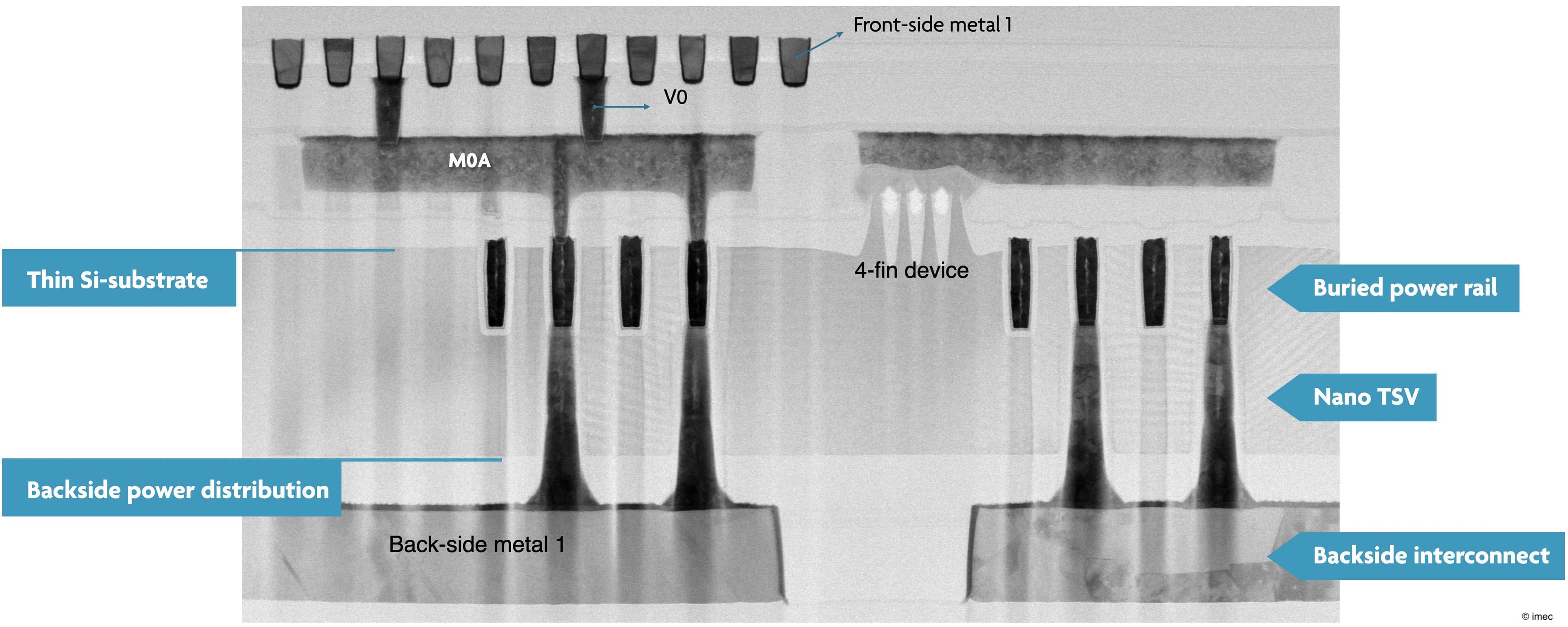
Figure 3 – TEM picture showing one specific implementation of a BSPDN. Power is brought from the backside to the FinFETs in the front side through nano-TSVs that land on a buried power rail.
The impact of Si substrate thinning: degraded failure current and inefficient heat dissipation
Imec investigated through measurement and simulation the impact of extreme Si substrate thinning (i.e., from 700µm to 300nm) on the performance of various ESD protection devices made in FinFET technology. These include STI and gated diodes, off-state MOSFETs (more specifically, GGNMOS), and on-state MOSFETs (more specifically, power-rail clamps). The performance of the various devices is mainly reflected by their failure current (It2, the current threshold for damage), a metric derived from TLP- and VF-TLP I-V curves. The team also explored the impact of substrate thinning on heat dissipation by simulating the lattice temperatures. These results were presented at the 2023 IEEE International Electron Devices Meeting (IEDM 2023) [2].
In general, ESD protection devices with thin Si substrates show reduced ESD robustness due to less efficient thermal dissipation. Devices with extremely thinned substrate show a reduction of the failure current with 20 - 40% compared to thicker variants. For STI diodes, for example, 100ns TLP It2 can be degraded by ~36% when the substrate is thinned from 700µm to 300nm. In simulations, a ~2x higher current density is observed throughout the 300nm Si substrate compared to the thick STI diode. A smaller degradation (~20%) of VF-TLP It2 is measured as it has a smaller thermal diffusion length than 100ns TLP.
Figure 4 - 100ns TLP measurement results of the STI diodes with Si thicknesses of 700µm and 300nm (as presented at IEDM 2023).
Figure 5 - Simulation results of the STI diode under 0.67A TLP current for two Si thicknesses (300nm and 4.5µm). Diodes with thinned Si substrate show (a) higher current density and (b-c) higher lattice temperature compared to diodes with thicker substrates (as presented at IEDM 2023).
As expected, the power rail clamps are least affected by substrate thinning. These devices, which rely on on-state MOSFETs, discharge ESD current by channel conduction while the other devices rely more heavily on the substrate to discharge.
Exploiting the functional backside to resolve the thermal issue
One of the technologies that require extreme substrate thinning are backside power delivery networks (BSPDNs). With BSPDNs, the power is delivered through the wafer’s backside, as such decoupling the power delivery network from the signal and clock delivery network in the frontside. In one specific implementation of a BSPDN, also shown in figure 3, the power is brought from the backside to FinFETs in the front side through nano-TSVs that land on a buried power rail (BPR). At VLSI 2023, imec investigated the impact of this new routing style with double-sided connectivity of the FinFETs on ESD protection devices and presented guidelines for a better layout style [3].
A few years ago, imec proposed to broaden the concept of BSPDN and migrate other devices or functionalities to the backside – an approach referred to as active functional backside technology. When implemented in the backside, the selected devices can be connected through different routing schemes, including the double-sided connectivity. This also provides opportunities for ESD protection devices.
Imec was the first to propose vertical ESD diodes, fabricated using the active functional backside technology. The process flow is based on imec’s technology for realizing extremely thinned Si and double-sided connectivity with BSPDNs [4]. Additional process steps were added to realize vertical diode structures, allowing to move the anode terminal from the frontside to the backside. As demonstrated at VLSI 2022, the vertical ESD diodes could significantly reduce layout area by 67% compared to ESD diodes with frontside connectivity only [5]. Also, the researchers experimentally observed increased ESD robustness thanks to enhanced current uniformity.
Figure 6 – (a-b) Process flow for fabricating vertical FinFET-based diodes with double-sided connectivity; (c) simulation structure of the vertical diode for thermal investigation (as presented at IEDM 2023).
At IEDM 2023, the imec researchers presented the very first study of the thermal behavior of these vertical ESD diodes and broadened their research to other types of ESD devices [2]. They investigated whether backside contacts and backside metallization layers dissipate heat more efficiently than if only frontside metallization was used. Simulations confirmed that these features can indeed ease the hot spots in various ESD devices. They could also impact the electrical characteristics of the ESD devices. But overall, these results make ESD devices with active backside contacts and metallization promising candidates for advanced technologies that rely on extreme Si substrate thinning.
Conclusion
Each new technology entering the semiconductor technology roadmap may present challenges and opportunities for ESD protection devices. The focus of this article was on the impact of Si substrate thinning, an enabling technology for BSPDN and advanced 3D integration technologies. The authors drew two major conclusions. First, thinned Si substrates degrade the ESD robustness of diode- and MOSFET-based ESD devices due to worse heat dissipation. Second, the active functional backside with double-sided connectivity presents opportunities for building more robust ESD protection devices.
This article was originally published in Semiconductor Digest.
Want to know more?
[1] ‘Next to FinFET, how will ESD suffer?’, ESD Association, blogpost by imec, July 2021
[2] ‘ESD challenges in 300nm Si substrate of DTCO/STCO scaling options,’ W.-C. Chen et al., IEDM 2023
[3] ‘Upcoming challenges of ESD reliability in DTCO with BS-PDN routing via BPRs’, W.-C. Chen et al., VLSI 2023
[4] ‘How to power chips from the backside: benefits and building blocks of a backside power delivery network,’ imec Reading Room.
[5] ‘Enabling active backside technology for ESD and LU reliability in DTCO/STCO,’ K. Serbulova et al., VLSI 2022
Interested in receiving the VLSI and IEDM papers? Fill in our contact form.

Wen-Chieh Chen received the B.S. and M.Sc. degrees from National Chiao-Tung University, Hsinchu, Taiwan, in 2016 and 2018, respectively. She is currently pursuing the doctoral degree with KU Leuven, Leuven, Belgium. She joined imec’s ESD team, in 2019 as a PhD student. Her research interests include mixed-voltage I/O circuit design and ESD device characterization in advanced sub-5nm technologies and DTCO/STCO era.

Marko Simicic received the B.Sc. and M.Sc. degrees in electrical engineering and information technology from the University of Zagreb, Croatia, in 2010 and 2012 respectively. He obtained a PhD degree from the department of electrical engineering ESAT, KU Leuven, Belgium in 2018. In 2017 he joined the ESD team in imec, Belgium. He is a certified ESD control program manager since 2022. He has authored or co-authored more than 35 papers in international journals and conference proceedings. His current research area is rather wide and includes ESD device and circuit design in advanced semiconductor and 3D/2.5D stacking technologies, novel ESD testing and ESD control process assessment.

Shih-Hung Chen (Masters 2002; PhD 2009) has been with the Device Reliability and Electric Characterization (DRE) Group at imec since 2010, and as ESD team lead and principal member of technical staff (PMTS) since 2019. He authored or co-authored more than 100 conference and journal publications. His current research interests include ESD protections in advanced sub-5nm technology nodes, in 3D/2.5D IC applications, and in Design Technology Co-Optimization (DTCO), System Technology Co-Optimization (STCO) with the integrations of III-V compounds.
Published on:
8 February 2024


