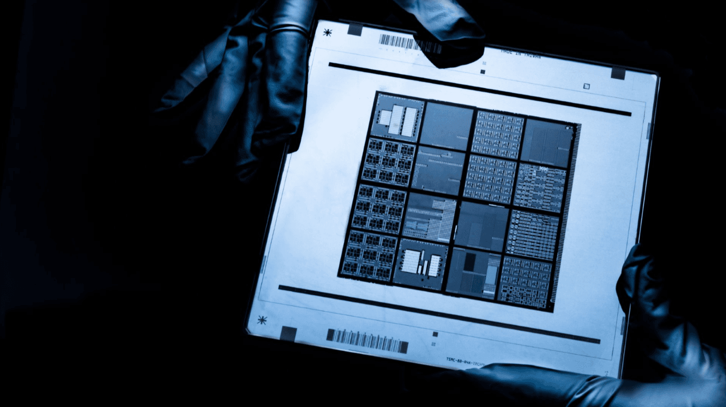
Inline metrology and materials characterization
To support the search for new device architectures with novel materials, imec develops analytical capabilities, whether for materials characterization or inline metrology.
Imec’s materials and components analysis and inline metrology expertise centers support imec’s ongoing R&D.
At the same time, they identify the innovative analytical capabilities that will be needed for tomorrow’s CMOS and post-CMOS semiconductor industry. If possible, they already implement them.
All according to our motto: “If you cannot see it, you cannot develop and control it.”
Materials and components analysis
This expertise center supports the development of tomorrow’s process flows for IC fabrication. We provide offline analytical feedback and develop the new characterization techniques that will be required.
The tools and techniques that we have cover the complete state of the art. They include APT, TEM, STEM, SEM, FIB, SPM, Raman PL, XPS, UPS, HAXPES, SIMS, RBS and ERD. This capacity is further supported by synchrotron-based analysis carried out at sites such as DIAMOND, BESSY, Soliel, ...
Within the European Graphene Flagship research initiative, we're working on bringing 2D materials from lab to fab.
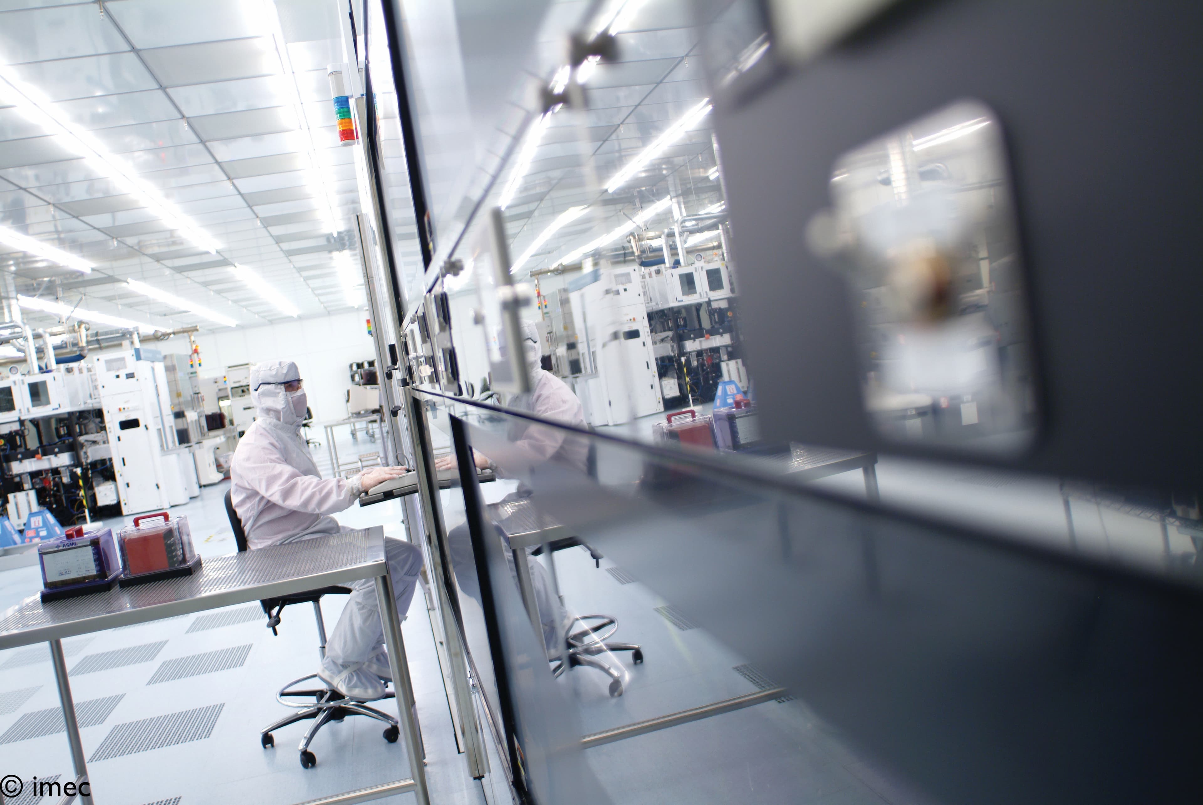
Inline metrology
Our inline metrology center ensures that process flows for semiconductor fabrication run as designed.
With the latest EUV lithography roadmap continuously pushing the boundaries of what is possible, we must also continuously develop new capabilities – often also a boost for lab-to-fab initiatives.
Another challenge we continue to work through is the ever-increasing data volume generated by a larger volume of smaller and more complex structures.
Introducing the AttoLab
Advancements in patterning, along with the introduction of 2D materials (which are already appearing on device scaling roadmaps) are needed to support the continued downscaling implied by Moore’s law. With this in mind, imec started in 2019 a joint development project with KMLabs and SPECS to create what is referred to as the AttoLab.
At the heart of the AttoLab are two table-top high harmonic generation (HHG) sources. HHG sources provide pulsed coherent photon beams enabling both interference lithography (IL) for patterning and a selection of characterization capabilities typically only found at synchrotron sites. See the characterization overview for more info.
These capabilities will support R&D topics including photoresist materials through to 2D materials. In addition, IL has already been demonstrated on the AttoLab down to 20 nm pitch, with plans to extend this to 8 nm.
Analytical capabilities to support tomorrow’s industry
Probably the biggest challenge will be to keep costs down while working with more complex structures and providing data faster.
Today, this is primarily supported via highly specialized techniques developed on mutually exclusive and costly platforms. Tomorrow’s solutions will include parallelization: synchronous measurements of potentially thousands of locations across a wafer. In this evolution, machine learning will be critical.
Want to know more?